SBAU382A November 2021 – January 2022 ADS7029-Q1 , ADS7039-Q1 , ADS7040 , ADS7041 , ADS7042 , ADS7043 , ADS7044 , ADS7046 , ADS7047 , ADS7049-Q1 , ADS7052 , ADS7054 , ADS7056 , ADS7057
2.2 Power Supplies
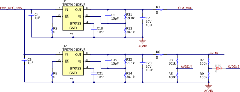
The default state of the EVM has all power supplies derived from the USB power and delivered by the PHI controller. The 3.3-V ADC digital supply voltage (DVDD) is provided by the PHI via pin 50 on J4 (see Figure 2-7). The PHI also provides a regulated 5.5-V power rail that feeds into two LDOs on the EVM. These LDOs generate a low-noise, 3.6-V (nominal) supply voltage for the amplifier (OPA_VDD) and a low-noise, 3.3-V (nominal) analog supply voltage for the ADC (AVDD). Figure 2-4 shows the two LDO circuits used on the ADS704X-5XEVM.
 Figure 2-4 Power Tree on the ADS704X-5XEVM
In Figure 2-4, the top LDO (U1) has an adjustable output set by resistors R31 and R32 while the bottom LDO (U2) has an adjustable output set by resistors R33 and R34. Modify these resistor values if a different OPA_VDD or AVDD voltage is desired. Ensure that the input, absolute, and common-mode voltage limitations for all components are within data sheet limits when modifying the power supplies. See the LDO data sheet for more information on how to choose resistor values for a specific output voltage.
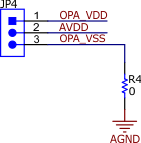
If external power supplies are desired, remove resistors R1 and R6 in Figure 2-4 to disconnect both LDOs from the power-supply circuit. Connector JP4 in Figure 2-5 can then be used to provide direct power to OPA_VDD, AVDD, and OPA_VSS.
 Figure 2-5 External Power-Supply Header on the ADS704X-5XEVM
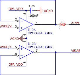
If OPA_VSS is connected to any voltage other than AGND, remove R4 in Figure 2-5 and replace R43 and R44 per the instructions in Figure 2-2. Another important consideration if OPA_VSS is modified is that the V– input (pin 4) on the buffer amplifier in Figure 2-6 is hard-wired to AGND and is therefore unaffected when the voltage on OPA_VSS is changed.
 Figure 2-6 Buffer Amplifier Circuit on the ADS704X-5XEVM
The buffer amplifier in Figure 2-6 prevents the AVDD/4 resistor divider (R3 and R5) from loading the amplifier inputs and the AVDD/2 resistor divider (R7 and R9) from loading the ADC inputs (see Figure 2-4). As per Section 2.1.1, VBIAS sets the driver amplifier common-mode voltage for both signal paths. AINM is only required if U3 or U5 in Figure 2-2 is populated with the ADS7043. This specific ADC has a pseudo-differential input that requires the AINM pin to be set to AVDD / 2 ±100 mV.
When the ADS7043 is used on the ADS704X-5XEVM:
- Populate R39 in Figure 2-4 with a 0-Ω resistor
- Populate R45 in Figure 2-6 with a 0-Ω resistor
- Depopulate R40 in Figure 2-2