SBAU412A November 2022 – May 2024 AFE7900 , AFE7903 , AFE7906 , AFE7920 , AFE7921 , AFE7950
- 1
- Abstract
- Trademarks
- 1 Introduction
- 2 Prerequisites
- 3 Typical Bare-Metal Design Flow
- 4 Background
- 5 Add Microblaze and SPI IP for Use in Vitis for Embedded Development
- 6 Create New Platforms in Vitis
- 7 Create New Application Projects in Vitis
- 8 Build Application Projects
- 9 Generate SPI Log for AFE79xx EVM
- 10AFE79xxEVM Board Modifications
- 11Configure the AXI GPIO
- 12Configure the AXI SPI
- 13Set Up and Power on Hardware
- 14Set up ZCU102 Board Interface for VADJ_FMC
- 15Debug Application Projects and Set up Vitis Serial Terminal
- 16Execute the Application
- 17Revision History
5 Add Microblaze and SPI IP for Use in Vitis for Embedded Development
- Open an existing Vivado project or create a new one.
- Under the ‘IP Integrator’ in the
left pane, click ‘Create Block Design’.
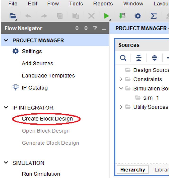 Figure 5-1 Creating Block
Design
 - Give a name to the block design
and click ‘OK’.
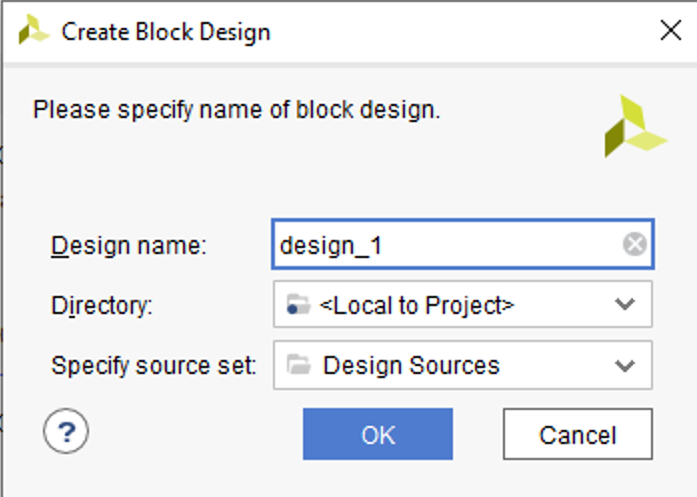 Figure 5-2 Name the Block
Design
 - In the newly created block
design, click ‘+’ to add IP.
 Figure 5-3 Adding IP to Block
Design
 - Search
for Microblaze and add ‘Microblaze’ to block design.
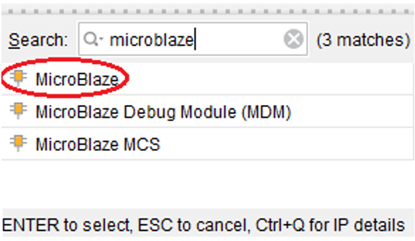 Figure 5-4 Adding Microblaze to
Block Design
 - Click ‘Run Block automation’ and
then ‘OK’.
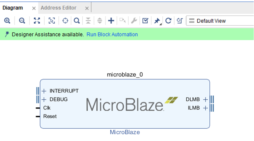 Figure 5-5 Run Block Automation
for Microblaze
 - Several IP blocks companions to Microblaze are automatically added by Vivado.
- Click ‘Run Connection automation’.
- In the Connection Automation
pop-up, select ‘CLK_IN1_D’, map it to ‘user_si570_sysclk’ and click ‘OK’.
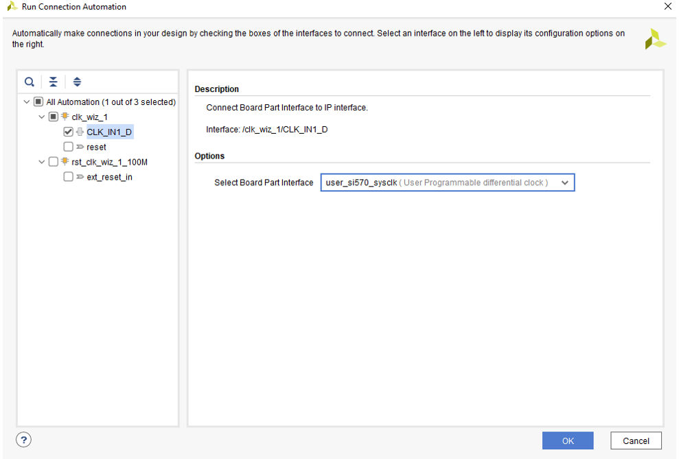 Figure 5-6 CLKIN for
Microblaze
 - Click ‘Run Connection automation’ again.
- In the Connection Automation
pop-up, select ‘reset’, ‘ext_reset_in’ and map them to ‘reset (FPGA_reset)’ and
click ‘OK’.
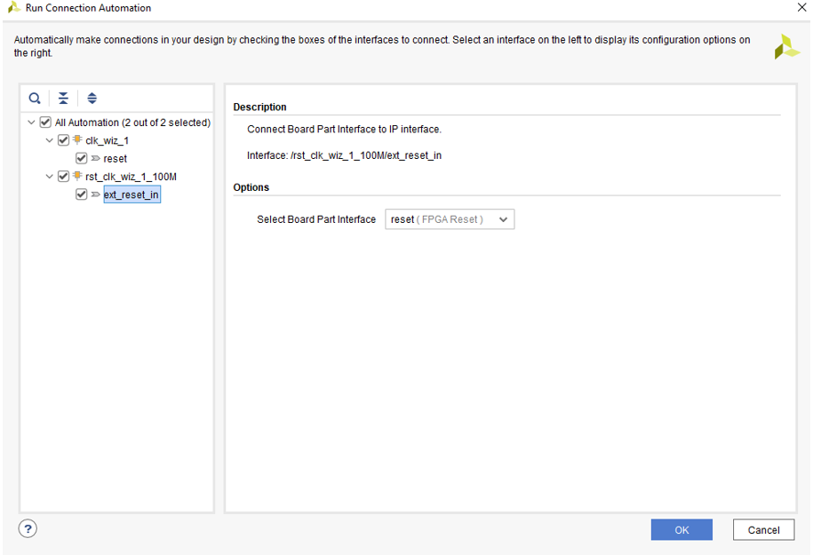 Figure 5-7 Reset Connection for
Microblaze
 - Right click block design and add
‘AXI Quad SPI’ as shown in Figure 5-8 and Figure 5-9.
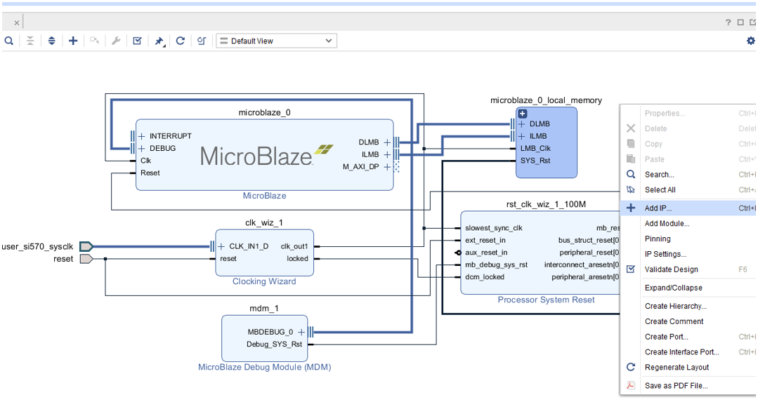 Figure 5-8 Adding IP to Block
Design
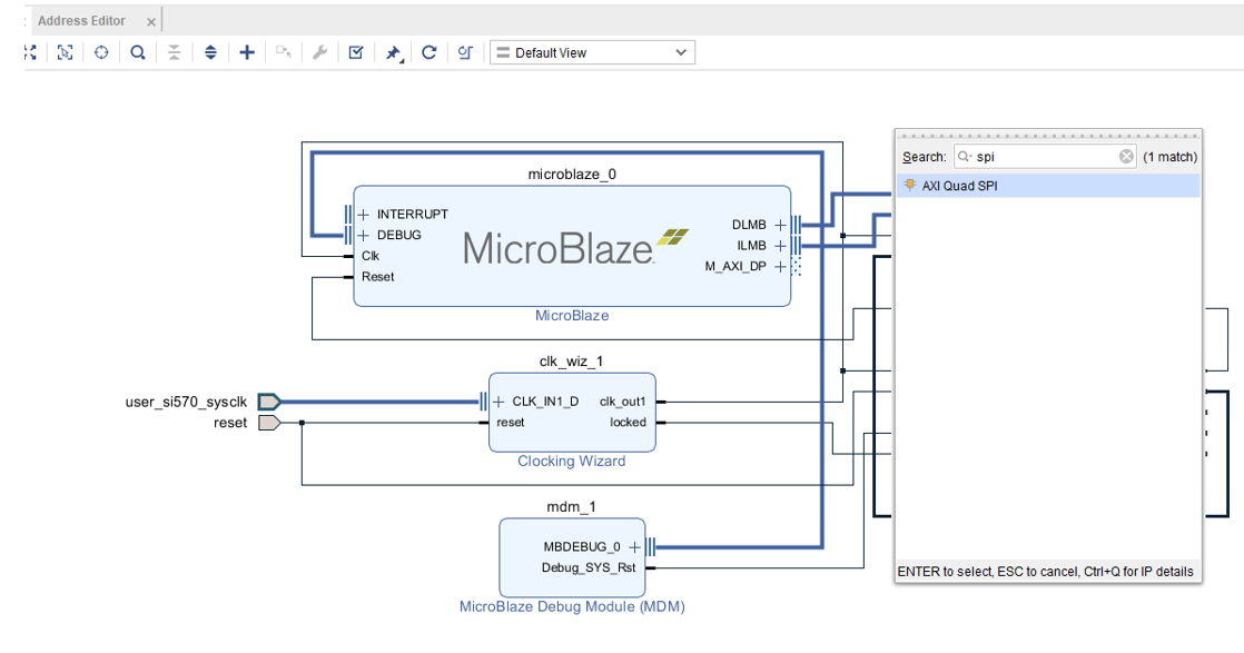 Figure 5-9 Adding ‘AXI QUAD SPI’
IP to Block Design
 - Click ‘Run Connection
automation’.
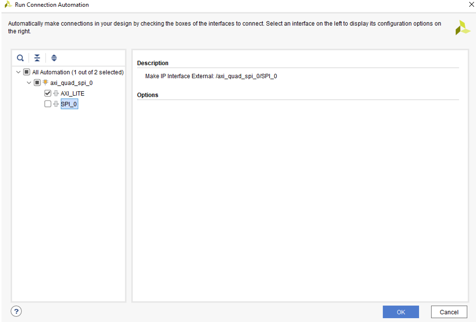 Figure 5-10 Running Connection
Automation for ‘AXI_LITE’
 - Select
‘AXI_LITE’ and click ‘OK’.
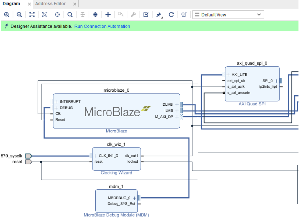 Figure 5-11 ‘ext_spi_clk’ Shows No
Connection in ‘AXI QUAD SPI’
 - Connect ‘s_axi_aclk’ to
‘ext_spi_clk’.
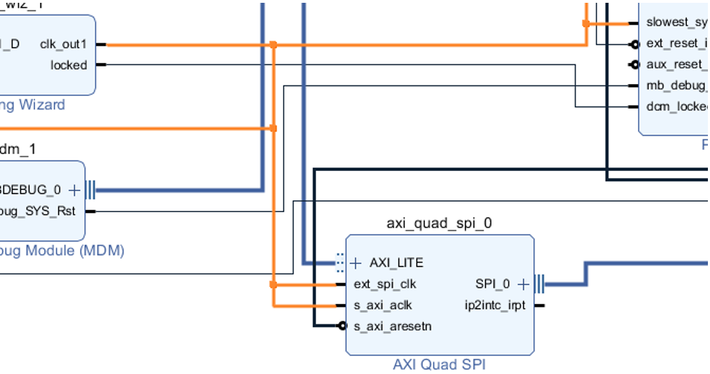 Figure 5-12 ‘ext_spi_clk’
Connected to ‘s_axi_aclk’
 - Double
click ‘AXI Quad SPI’ -> select No. of slaves and then click ‘OK’.
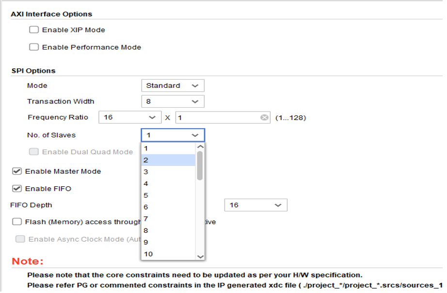 Figure 5-13 Select Number of SPI
Slaves in ‘AXI QUAD SPI’
 - From the Quad SPI IP, map the
signals as following:
- ‘io0_o’ -> SPI_SDO
- ‘Io1_i’ <- SPI_SDI
- ‘sck_o’ -> SPI_SCL
- ‘ss_o[1:0] -> SPI_SEN0, SPI_SEN1
- The ‘ss_o’ bit width will be
based on No. of slaves selected in step:16
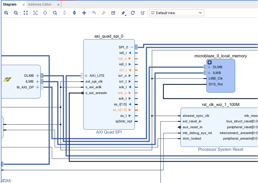 Figure 5-14 Highlighting Ports for
External Connections in ‘AXI QUAD SPI’
 - Validate
the design to ensure no errors as shown in Figure 5-15.
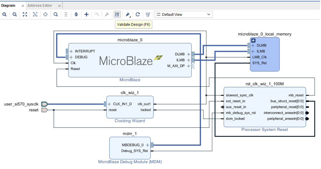 Figure 5-15 Validating Block
Design
 - To add GPIOs, add ‘AXI GPIO’ from catalog and repeat similar steps as above.