SBOA542 November 2022 TMP1826 , TMP1827
2.6 Software Driver for SPI
The following code shows a generic SPU configuration for 8-bit data and mode-1 of operation with SPI clock rate of 100500 Hz.
void ConfigureSPI()
{
    // Configure SPI for 8-bit data, CPOL=0 and CPHA=1
    SPIConfig(DATA_8_BIT, CPOL_0, CPHA_1);
    SPIDataRate(100500);
}
The following pseudocode shows how to implement bus reset and response. As the previous state of the bus communication can be write or read of data over the single-wire interface, TI recommends that the SPI clock rate be explicitly configured before bus reset and response is executed.
void mcu_txOneWireReset()
{
    // Configure SPI clock speed 100,500 Hz
    SPIDataRate(100500);
    // Send Bus Reset on SPI.DOUT transmit pin
    SPISendData(0x07);
    // Wait for Response on SPI.DIN pin
    while(SPIGetData() != 0x05);
    // Configure SPI clock speed 500,000 Hz
    SPIDataRate(500000);
}
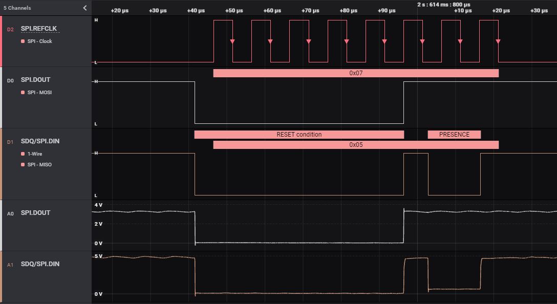
For the previously-described application example code, Figure 2-15 illustrates the bus transactions along with an SPI frame. The host sends 0h07 for bus reset (indicated by marker 0) and the device responds to the reset (indicated by marker 1) with a response of 0h05.
 Figure 2-15 Scope Capture of Bus Reset and Response
Once the bus reset is sent and a response received, the host then sends the address command and function command to the device. As all commands and data transfers are at byte boundary, the pseudocode shows how to send the bytes and bits to the device.
void mcu_txOneWireByte(uint8_t bytevalue)
{
    uint8_t count;
    // Shift bits LSB to MSB
    for(count=0; count<8; count++)
    {
        mcu_txOneWireBit((bytevalue >> count) & 0x01);
    }
}

void mcu_txOneWireBit(uint8_t bitvalue)
{
    // If logic '0' then send 0xF0
    if(bitvalue == 0x00)
    {
        SPISendData(0x01);
    }
    // If logic '1' then send 0xFF
    else if(bitvalue == 0x01)
    {
        SPISendData(0x7F);
    }
}
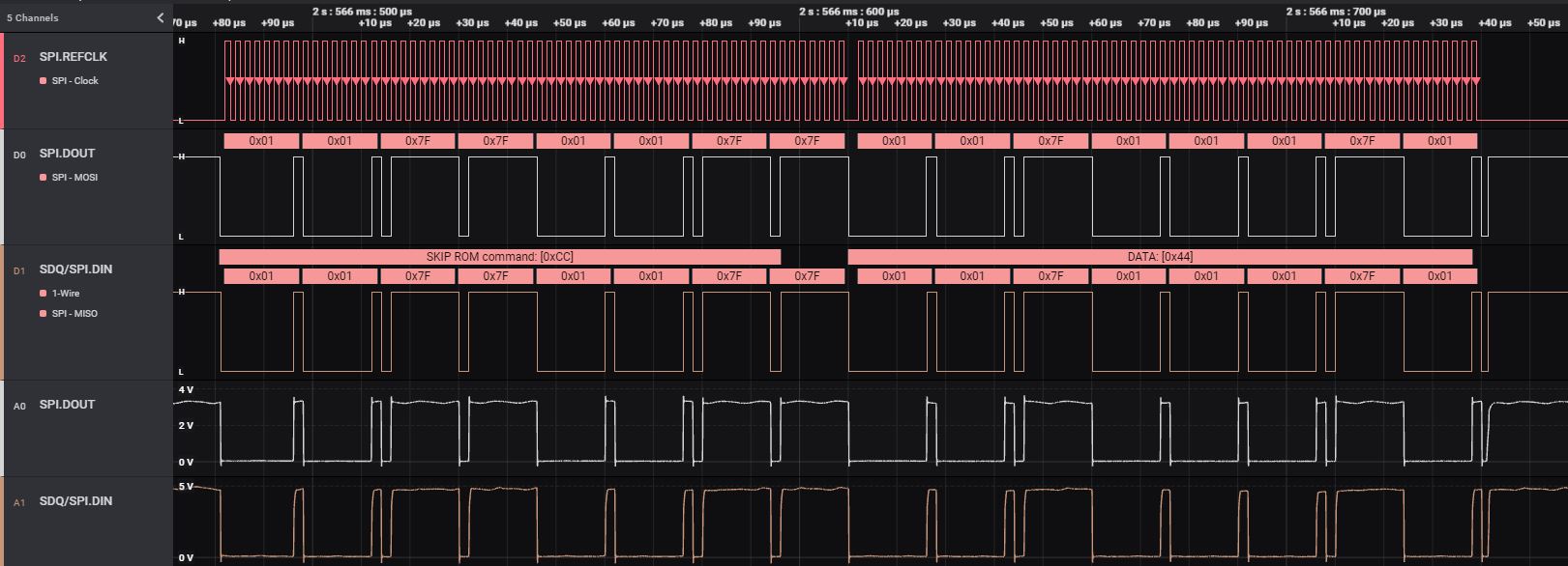
Figure 2-16 shows the write byte transfer of address command 0hCC (SKIPADDR) and function command 0h44 (CONVERTTEMP) for temperature conversion. During the write operation the SPI.DOUT is set as 0h01 and 0h7F to indicated a logic '0' and logic '1', respectively. Since the device is always in receive state, the device does not respond on the SDQ pin and hence the SPI.DIN pin mirrors the SPI.DOUT pin.
 Figure 2-16 Scope Capture of Write Transfer
The following pseudocode shows how to implement read from the device after sending an address or function command to which the device can respond. As with data transfer to the device, whenever data is read back from the device, the read is done at byte boundary. The following function shows how to implement both the byte and bit read functions.
uint8_t mcu_rxOneWireByte(void)
{
    uint8_t count;
    uint8_t rxbyte = 0x00;
    // Shift bits LSB to MSB
    for(count=0; count<8; count++)
    {
        rxbyte |= (mcu_rxOneWireBit() << count);
    }
}

uint8_t mcu_rxOneWireBit(void)
{
    uint8_t rcvbyte;

    // Send the Falling edge to begin the read
    SPISendData(0x7F);
    // Get the data from Receive pin
    rcvbyte = SPIGetData();

    if(rcvbyte == 0x7F)
    {
        return(1);
    }
    else
    {
        return(0);
    }
}
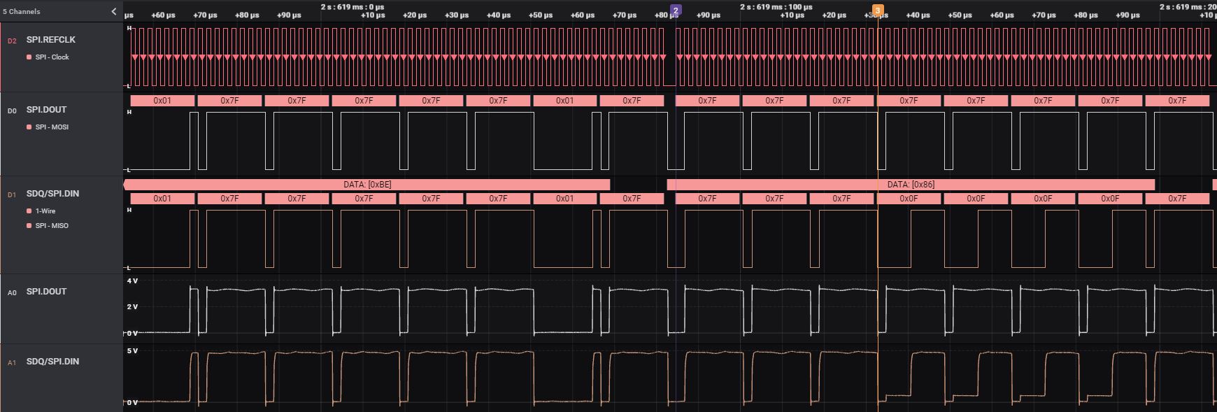
Figure 2-17 shows the write of the function command 0hBE (READ SCRATCHPAD-1) and the read byte that follows. The host during the read operation drives SPI.DOUT as 0h7F. As indicated by marker 2, if the device has a logic '1' to send to the host, the device does not drive the SDQ pin and the byte received by SPI.DIN is 0h7F. When the device has a logic '0' to send to the host, the device drives the SDQ pin low as shown by marker pair 3. The SPI.DIN pin of the host in this case receives a 0h0F.
 Figure 2-17 Scope Capture of Read Transfer