SBOU236A February 2020 – March 2021 ALM2403-Q1
5 Input and Output Connections
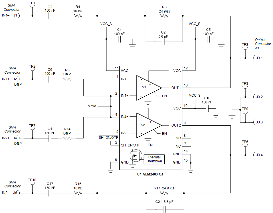
Input signal connections for the ALM2403Q1EVM are provided through the use of the SMA connectors and test points located at the left of the EVM. The dual output-amplifier connections are provided through connector J3 and test points located at the right side of the EVM. A simplified diagram of the ALM2403Q1EVM input and output connections is displayed in Figure 5-1.

Note: SMA
connectors J2 and J4 are not populated. Resistors R6 and R14 are not
populated.
Figure 5-1 ALM2403Q1EVM Input and Output ConnectionsTable 5-1 summarizes the input and output connectors and corresponding test points.
Table 5-1 ALM2403Q1EVM Input and Output Connections
| Connector Designator | Signal | Comment | Test Point |
|---|---|---|---|
| J1 | IN1– | SMA | TP1 |
| J2 | IN1+ | SMA (not populated) | TP2 |
| J4 | IN2+ | SMA (not populated) | TP7 |
| J6 | IN2– | SMA | TP10 |
| J3.1 | OUT1 | Screw terminal | TP3 |
| J3.2 | GND | Screw terminal | TP8 |
| J3.3 | GND | Screw terminal | TP9 |
| J3.4 | OUT2 | Screw terminal | TP6 |