SLUAA81A October 2020 – February 2022 BQ769142 , BQ76922 , BQ76942 , BQ76952
2.2 External Cell-Balancing Circuit Design Using N-Channel FETs
For applications that need higher cell balancing current, external FETs are often used. When using external FETs, the cell input resistors can be increased to the maximum recommended value of 100 Ω. Increasing the resistor size will help to provide enough voltage across the gate of the FET. In Figure 2-2, as the internal FET is turned on inside the device, the current flowing through Rn-1 provides the VGS for the external FET.
 Figure 2-2 Balancing Circuit Using External
N-channel FETs
Figure 2-2 Balancing Circuit Using External
N-channel FETsCare must be taken to select an external FET with a low RDSON defined at low VGS. For example, the default balancing minimum voltage defined by the parameter Cell Balance Min Cell V is 3900 mV. The external FET should have an RDSON defined at or below 3.9V x 100 / (100 + 100 + 25) = 1.73 V.
A Zener diode is needed to protect the external FET gate from pack transients. For example, in the event of a short across the pack in a 10-cell battery, Cell 10 would have approximately 40V across Rn during the event and the opposite transient at the release of the short circuit. The gate voltage should be connected through a resistor to limit the current when the diode conducts. (During normal operation the Zener will not conduct).
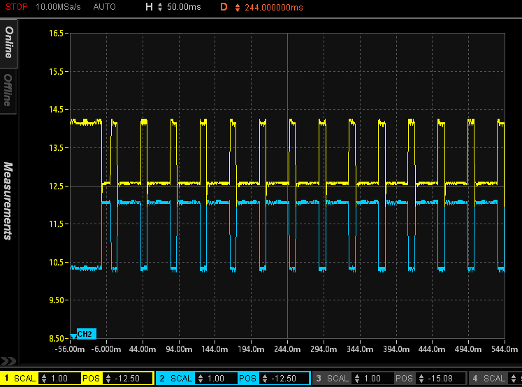
For the waveform captured below, the circuit was designed with an Rn of 100 Ω and Rgn of 1k Ω. The Rbal resistor is set to 50 Ω for a balance current of 80 mA through the external FET at 4V. At this cell voltage, an additional ~16 mA of current flows through the internal FET of the device for a total balancing current of close to 96 mA. An N-channel MOSFET was selected with an RDSON defined for low VGS down to 1.4V.
 Figure 2-3 BQ76942 Cell Balancing With N-Channel
FET, Cell 4 (yellow) = 3.7 V, Cell 3 (blue) = 3.5 V