SLUAAH0 February 2022 UCC14130-Q1 , UCC14131-Q1 , UCC14140-Q1 , UCC14141-Q1 , UCC14240-Q1 , UCC14241-Q1 , UCC14340-Q1 , UCC14341-Q1 , UCC15240-Q1 , UCC15241-Q1
- Trademarks
- 1 Introduction
- 2 Three-Phase Traction Inverter
- 3 Gate Drive Bias Requirements
- 4 Single Positive Isolated Output Voltage
- 5 Dual Positive and Negative Output Voltages
- 6 Dual Positive Output Voltages
- 7 Capacitor Selection
-
8 RLIM
Current Limit Resistor
- 8.1 RLIM Functional Description
- 8.2
RLIM
Dual Output Configuration
- 8.2.1 CVEE Above Nominal Value CVDD Below Nominal Value
- 8.2.2 CVEE Below Nominal Value CVDD Above Nominal Value
- 8.2.3 Gate Driver Quiescent Current: IQ_VEE > IQ_VDD
- 8.2.4 Gate Driver Quiescent Current: IQ_VEE < IQ_VDD
- 8.2.5 CVEE Above Nominal Value CVDD Below Nominal Value: IQ_VEE > IQ_VDD
- 8.2.6 CVEE Below Nominal Value CVDD Above Nominal Value: IQ_VEE < IQ_VDD
- 8.3 RLIM Single Output Configuration
- 9 UCC14240-Q1 Excel Design Calculator Tool
- 10Thermal Considerations
- 11Enable (ENA) and Power Good (/PG)
- 12PCB Layout Considerations
- 13Reference Design Example
- 14Summary
- 15References
3.5 Output Voltage Requirements
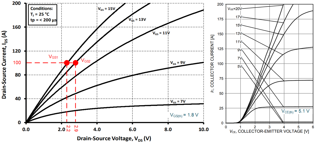
Another important differentiation between IGBTs and SiC MOSFETs is their ID, (IC) vs VDS, (VCE) output characteristics. The left curve in Figure 3-2 shows the ID vs VDS for a SiC MOSFET, while the right side depicts the IC vs VCE for an IGBT. Both are 1.2-kV rated devices.

Figure 3-2 1200 V, 100 A, SiC vs IGBT, VI Characteristics
The IGBT curves show a steep slope in the linear region and a slope of nearly zero in the saturation region. The transition between the linear, ohmic region and saturation region is sharp and distinct so that for any collector-emitter voltage greater than the threshold voltage, VCE(th), the IGBT appears as a voltage controlled current source.
Conversely, the SiC curves show no defined linear or saturation region and a much smaller change in ID vs VGS compared to the IGBT. As such, SiC MOSFETs are considered low or modest gain devices that are characterized by a continuous decrease in RDS(ON) up to the drain-source breakdown voltage. It is therefore, desirable to turn-on SiC MOSFETs with positive VGS applied as close as possible to their breakdown voltage. For example, consider the two operating points, VGS1 and VGS2, highlighted in the SiC IV curves of Figure 3-2.
Comparing the two operating points shows a 32% RDS(ON) increase and consequential conduction losses are 1.32 times higher when turning on with VGS2=13 V as opposed to VGS1=15 V. This behavior means the SiC acts more like a voltage-controlled resistor. The VDD turn-on bias supply should be tightly regulated to allow operation as close to 15 V as possible.
Some SiC MOSFET manufacturers recommend 5% accuracy on VDD but designers are often looking for 3% or even 1.5% VDD accuracy for traction inverter applications. Whether using power supply modules or a discrete design such as a distributed flyback converter, achieving such high regulation accuracy can be difficult and often requires additional post-regulation using low dropout (LDO) linear regulators. Better than 1.3% voltage regulation is one of the key features of UCC14240-Q1 making it well suited for enhancing SiC MOSFETs to their lowest RDS(ON) without the need for LDO’s or discrete post-regulation circuitry.
Another notable difference between IGBTs and SiC MOSFETs is the VGS(th) (VCE(th)) turn-on threshold voltage. For the two devices shown in Figure 3-2, this is noted in the lower right corner of each graph. SiC MOSFETs have low minimum VGS(th) and switch at high dV/dt making them more susceptible to dV/dt induced turn-on in half-bridge configurations. This is a condition where the low-side MOSFET of a half-bridge, such as those used in traction inverters, can inadvertently turn-on while VGS commands it to be in the off-state. One way to circumvent this is to apply a negative voltage during turn-off, providing additional margin against the low VGS(th). The UCC14240-Q1 provides a switched capacitor voltage to generate a regulated, negative VEE voltage for reliable turn-off of SiC and IGBT transistor switches. This is a necessary part of a gate driver bias solution for assuring robustness of the SiC or IGBT module in harsh automotive environments.