SLUAAT4 November 2023 TPS543320 , TPS543620 , TPS543820 , TPSM843320 , TPSM843620 , TPSM843820
2.1.2 PCB Design Size Comparison
The external components for both the TPS543620 and TPSM843620 PCB design size were selected based on data sheet recommendations for identical applications. The selected design parameters are shown in Table 2-1.
| Parameter | Value |
|---|---|
| Input voltage range (VIN) | 4 to 18 V, 12 V nominal |
| Output voltage (VOUT) | 1.0 V |
| Output current rating (IOUT) | 6 A |
| Switching Frequency (fSW) | 1000 kHz |
| Input Capacitance (CIN) | 20.2 µF |
| Output Capacitance (COUT) | 94 µF |
| Output Inductance (LOUT) | 470 nH |
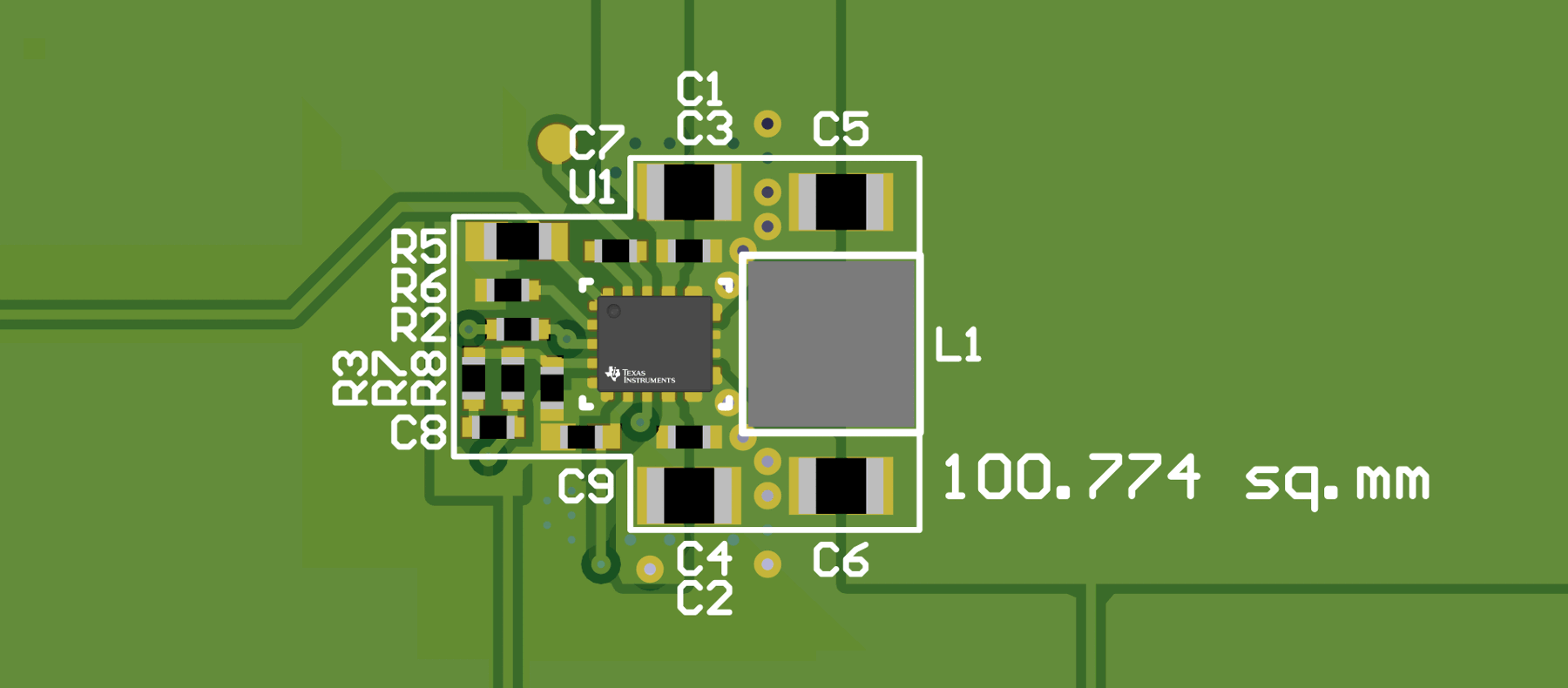
 Figure 2-2 TPS543620 PCB Design Size
The total design size of the TPS543620 converter circuit design was measured to be approximately 100.774 mm2.
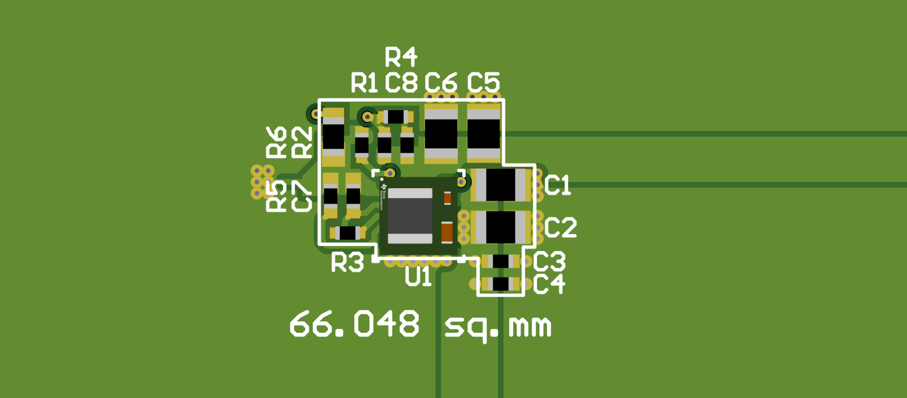
 Figure 2-3 TPSM843620 PCB Design Size
The total design size of the TPSM843620 module circuit design was measured to be approximately 66.048 mm2.
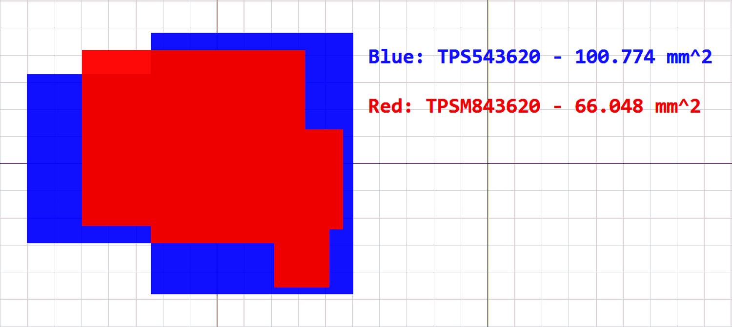
 Figure 2-4 PCB Design Size Overlay Comparison
When comparing the PCB design size of both the TPS543620 converter and the TPSM843620 module, it is clear that the module has a smaller design size than the converter by about 34.5%. This noticeable difference is because the module uses a small MicroSiP package and reduces the number of external components to significantly decrease the final design size.