SLVAE69 July 2019 TPS568215 , TPS56C215
2 12 V / 5 V O-ring supply for DDR application
In workstation DDR applications, customers can use 12 V to convert 2.5 V for Vpp supply. When 12 V fails, customers can have another 5 V rail as backup source to supply the Vpp rail. So customers typically want to use their ORing topology summing together 5 V and 12 V inputs to Vin through diodes. Considering the margin, usually a 4 V–13.2 V input range voltage buck converter is employed here. A simplified schematic is shown in Figure 2
 Figure 2. Simplified Schematic of DDR Vpp Supply
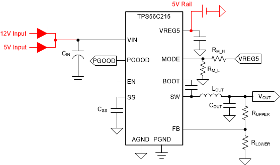
 In the current market, devices with 17 V max-VIN ratings typically have a minimum input voltage in the range of 4.5 V. If the VIN_min goes lower, the internal logic circuit power supply would be difficult to realize or the cost of device will increase significantly, especially for a high-current device. For this DDR application, there is already 5 V rail in the system. When connecting this 5 V to VREG5 for internal circuit supply, the buck converter could support input voltages lower than 4.5 V, meaning the customer could use the current solution to realize 5 V / 12 V ORing topology. The configuration schematic based on TPS56C215 is shown in Figure 3.
 Figure 3. Configuration Schematic Based on TPS56C215