SLVAFT0 July 2024 DRV8706-Q1 , DRV8714-Q1 , DRV8718-Q1
3.1 Example Measurements
Using a DRV8718-Q1 EVM, we can measure examples of the effect of bulk capacitance. We used a 50% duty cycle PWM signal with a 12V supply, and a load of 3 Ohms in series with a 470uH inductor to simulate a typical DC motor circuit. The L/R time constant is 157 microseconds, about three times the PWM period.
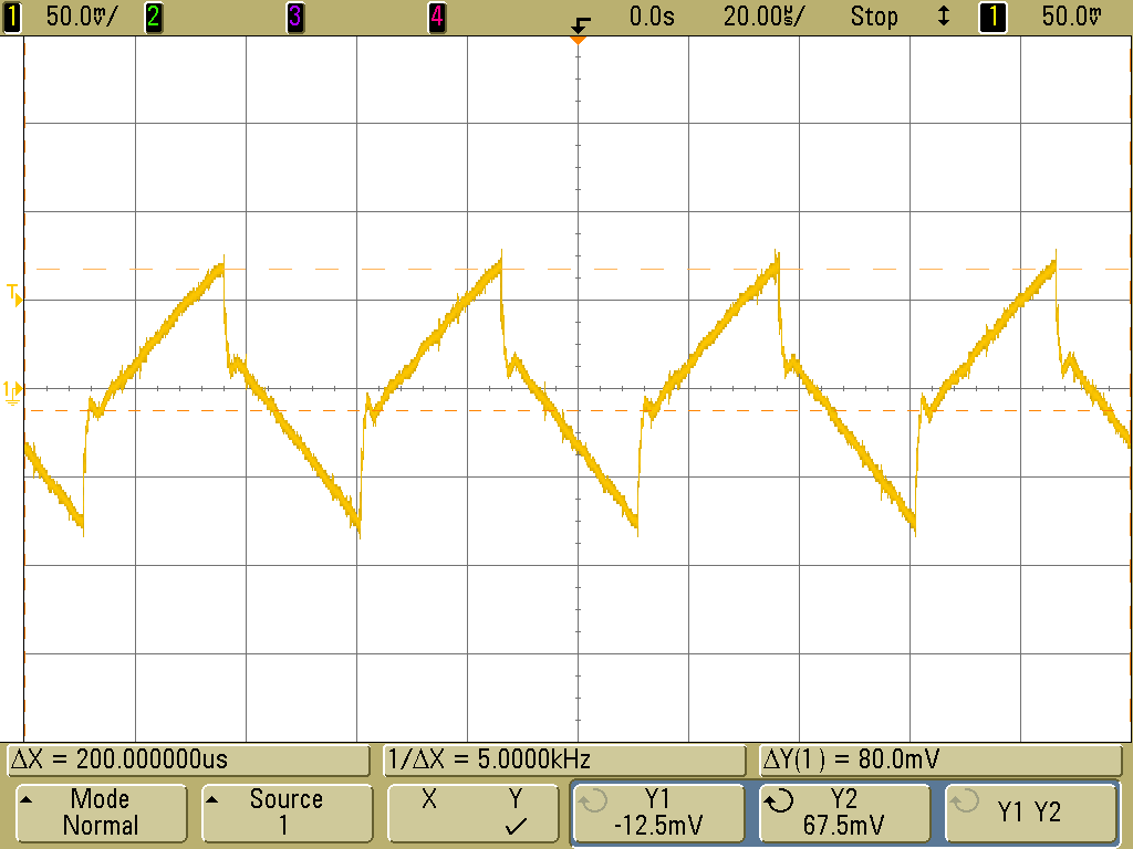
Figure 3-1 shows the case where the bulk capacitance is 270uF. Using the estimate for ideal capacitors, we can expect about 80mV of variation in PVDD due to the capacitor charging and discharging during PWM. Neglecting the quick shift during each transition, the voltage ramp does have an amplitude of about 80mV, as indicated by the dashed cursors.
However, the total variation in PVDD in Figure 3-1 is about160 mV, significantly more than predicted by the ideal capacitor estimate. There is a sharp shift in the voltage at the beginning of each transition, which is due to the non-ideal properties of the bulk capacitors. The equivalent series resistance (ESR) of electrolytic capacitors can account for this quick voltage shift.
 Figure 3-1 PVDD Variation With 270uF Bulk
Capacitance, Measured Results During PWM
Figure 3-1 PVDD Variation With 270uF Bulk
Capacitance, Measured Results During PWMThe variation on PVDD consists of mainly two components, the voltage due to the charging and discharging of the bulk capacitance, and the voltage across the non-ideal equivalent series resistance (ESR) of the capacitors.
The equivalent series resistance (ESR) of real capacitors is one measure of how non-ideal their characteristics are. Low ESR capacitors are typically more expensive, but can provide benefits in terms of reduced voltage ripple. This is a common topic in power supply design, for example, see the Output Ripple Voltage for Buck Switching Regulator, application note.
With simulation, we can see what the ripple looks like with an ideal capacitor having zero ESR, and also model the real-world capacitor by adding a resistance in series to represent the ESR.
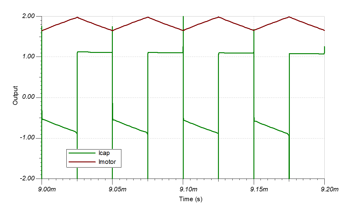
First let us look at how the current flows in the capacitor, and thus how the voltage varies across the ESR we model as part of the capacitor. During the 'on' part of the PWM cycle, the capacitor acts as a source of motor current, so the voltage drop across the ESR subtracts from the internal ideal voltage stored in the capacitor. Thus the voltage across the capacitor, including the ESR, is lower than the internally stored voltage. During the off' part of the PWM cycle, the capacitor acts as a current sink, charging up the internal voltage. During this charging, the voltage across the capacitor, including the ESR is higher than the internally stored voltage. The motor and capacitor currents are shown in Figure 3-2.
 Figure 3-2 Motor Current (Red) and
Capacitor Current (Green) During PWM
Figure 3-2 Motor Current (Red) and
Capacitor Current (Green) During PWMIn Figure 3-3 a TINA simulation shows the voltage variation due to PWM of the MOSFET T1, with a bulk capacitance of 270uF and zero ESR, modeling an ideal capacitor. The voltage variation on PVDD is about 100mV. Figure 3-3 simulation largely agrees with the ideal capacitance equations.
 Figure 3-3 TINA Simulation with Zero
ESR
 Figure 3-4 TINA Simulation With 50mΩ
ESR
Figure 3-4 TINA Simulation With 50mΩ
ESRNote how adding ESR makes the waveform look more like the actual results.
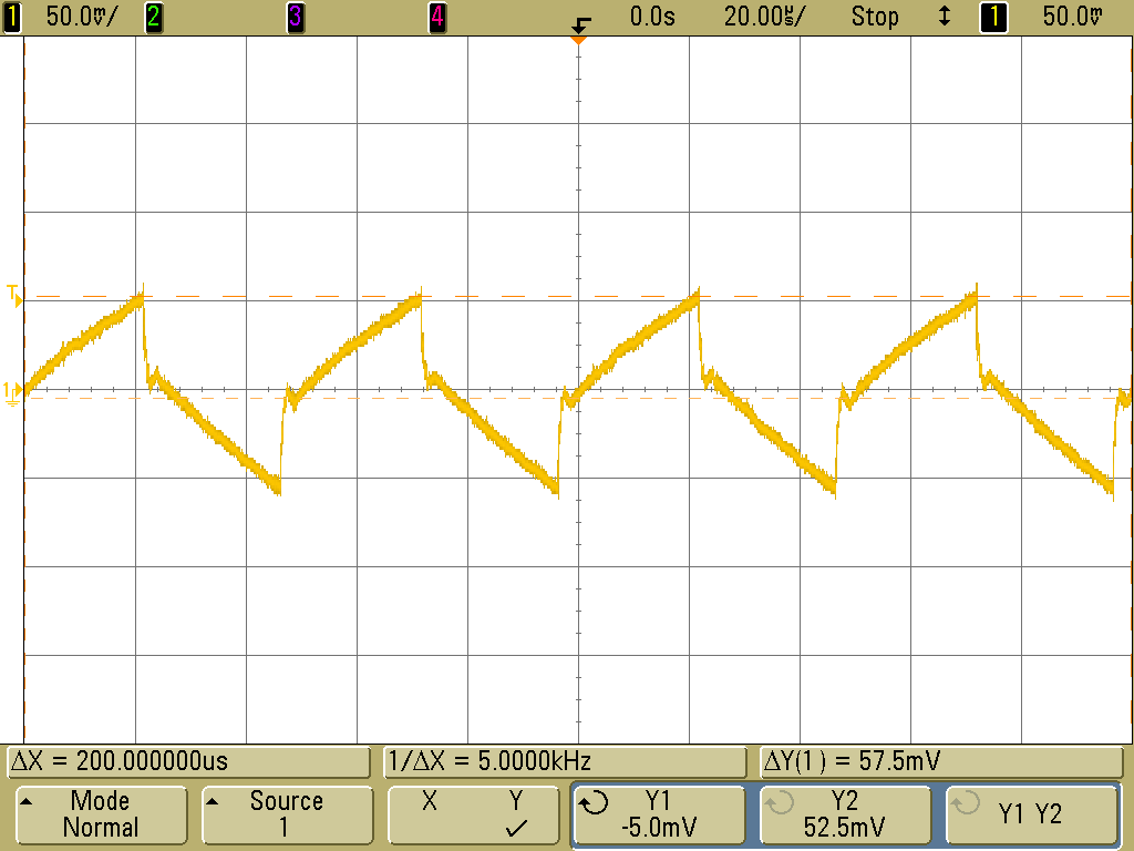
Another real-world case is shown in Figure 3-5 where the bulk capacitance has been increased to 600uF by adding a 330uF capacitor in parallel with the 270uF of the previous case. The ideal capacitor estimate given previously can predict a voltage variation of about 36mV. The measured value is about 57mV; so while the voltage variation has been reduced by adding more bulk capacitance, it has not been reduced as much as predicted by the ideal estimate.
 Figure 3-5 PVDD Variation With 600uF Bulk
Capacitance
Figure 3-5 PVDD Variation With 600uF Bulk
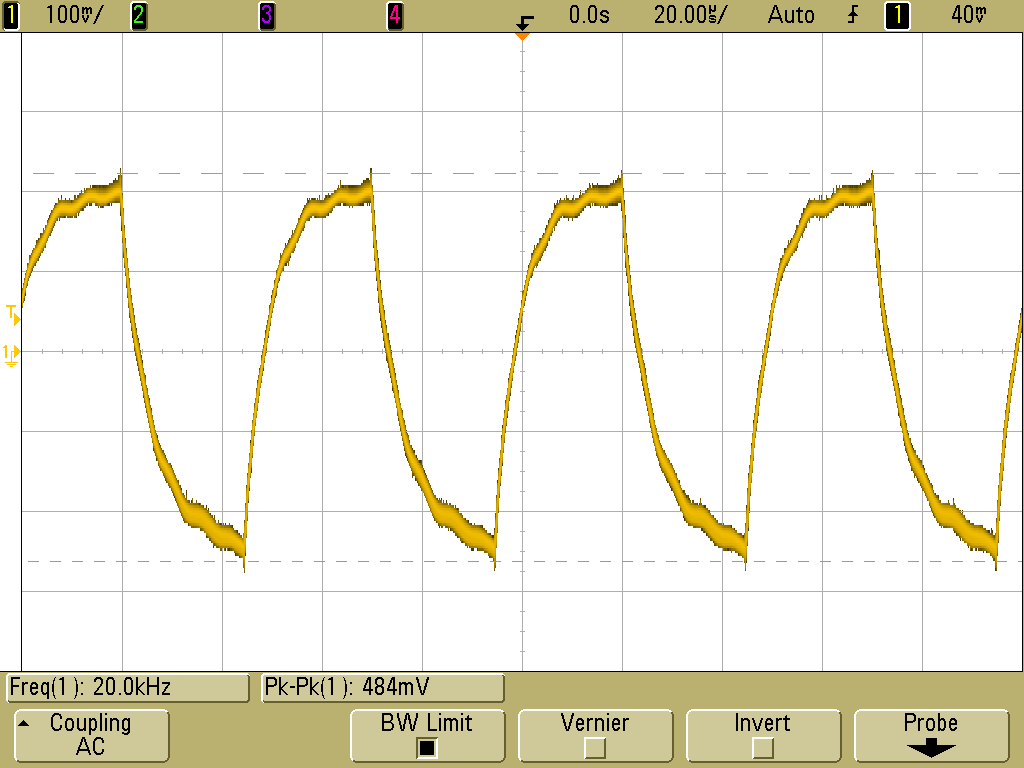
CapacitanceFigure 3-6 shows one more example, with the bulk capacitance reduced to 120uF. Now the voltage ripple increases to almost 500mV, and the shape is dominated by the charging and discharging of the capacitance, and the effect of the ESR is less evident.
 Figure 3-6 PVDD Variation With 120uF Bulk
Capacitance