SLVUAK9A December 2015 – May 2021 TPS65265
4.1 Header Description and Jumper Placement
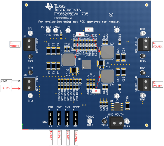
Figure 4-1 shows the jumper and pin placement on the TPS65265EVM-705 board.
 Figure 4-1 TPS65265EVM-705 Header Description and Jumper Placement
Test points:
- LX of VOUT1
- LX of VOUT2
- LX of VOUT3
VOUT1, VOUT2, VOUT3, VIN, PGOOD, PG_DLY, SYNC
Table 4-1 Input/Output Connection
| # | Function | Description |
|---|---|---|
| J1 | Buck1 Connector | Output of Buck1 |
| J2 | Buck2 Connector | Output of Buck2 |
| J3 | Buck3 Connector | Output of Buck3 |
| J5 | VIN Connector | Apply power supply to this connector |
Table 4-2 Jumpers
| # | Function | Placement | Comment |
|---|---|---|---|
| J6 | Buck1 enable (EN1) | Connect EN1 to GND to disable VOUT1 Connect EN1 to HIGH or leave open to enable VOUT1 | |
| J7 | Buck2 enable (EN2) | Connect EN2 to GND to disable VOUT2 Connect EN2 to HIGH or leave open to enable VOUT2 | |
| J8 | Buck3 enable (EN3) | Connect EN3 to GND to disable VOUT3 Connect EN3 to HIGH or leave open to enable VOUT3 | |
| J9 | MODE | Power sequencing mode control pin. Connect MODE pin to GND or HIGH, set the power sequence with pre-defined power up and power down sequence. Leave open to set power up and down with dedicated enable pin. |