SLVUCZ9 July   2024 DRV81004-Q1 , DRV81008-Q1 , DRV81620-Q1


  1.   1
  2.   Description
  3.   Get Started
  4.   Features
  5.   Applications
  6.   6
  7. 1Evaluation Module Overview
    1. 1.1 Introduction
    2. 1.2 Kit Contents
    3. 1.3 Specification
    4. 1.4 Device Information
  8. 2Hardware
    1. 2.1 Header Information
    2. 2.2 Connector and Jumper Information
    3. 2.3 Hardware Setup
  9. 3Software
    1. 3.1 Software Setup
    2. 3.2 Web GUI Access or Local GUI Installation
    3. 3.3 Connecting EVM to GUI
    4. 3.4 GUI Overview
      1. 3.4.1 Low-Side Drivers: DRV81004-Q1 and DRV81008-Q1
      2. 3.4.2 High-Side Driver: DRV81080-Q1
      3. 3.4.3 Configurable HS/LS: DRV81602-Q1, DRV81242-Q1, and DRV81620-Q1
  10. 4Hardware Design Files
    1. 4.1 Schematics
    2. 4.2 PCB Layouts
    3. 4.3 Bill of Materials (BOM)
  11. 5Additional Information
    1. 5.1 Known Hardware or Software Issues
    2. 5.2 Trademarks

Configurable HS/LS: DRV81602-Q1, DRV81242-Q1, and DRV81620-Q1

The DRV81602-Q1, DRV81242-Q1, and DRV81620-Q1 are configurable high-side and low-side drivers with integrated protection and diagnostics. The configurable driver GUIs are set up in the same configuration and offers many of the same features and functionalities as the DRV81080-Q1 high-side driver. Minor differences include exclusion of Enabling OLON Diagnostics for dedicated low-side drivers in certain variants.
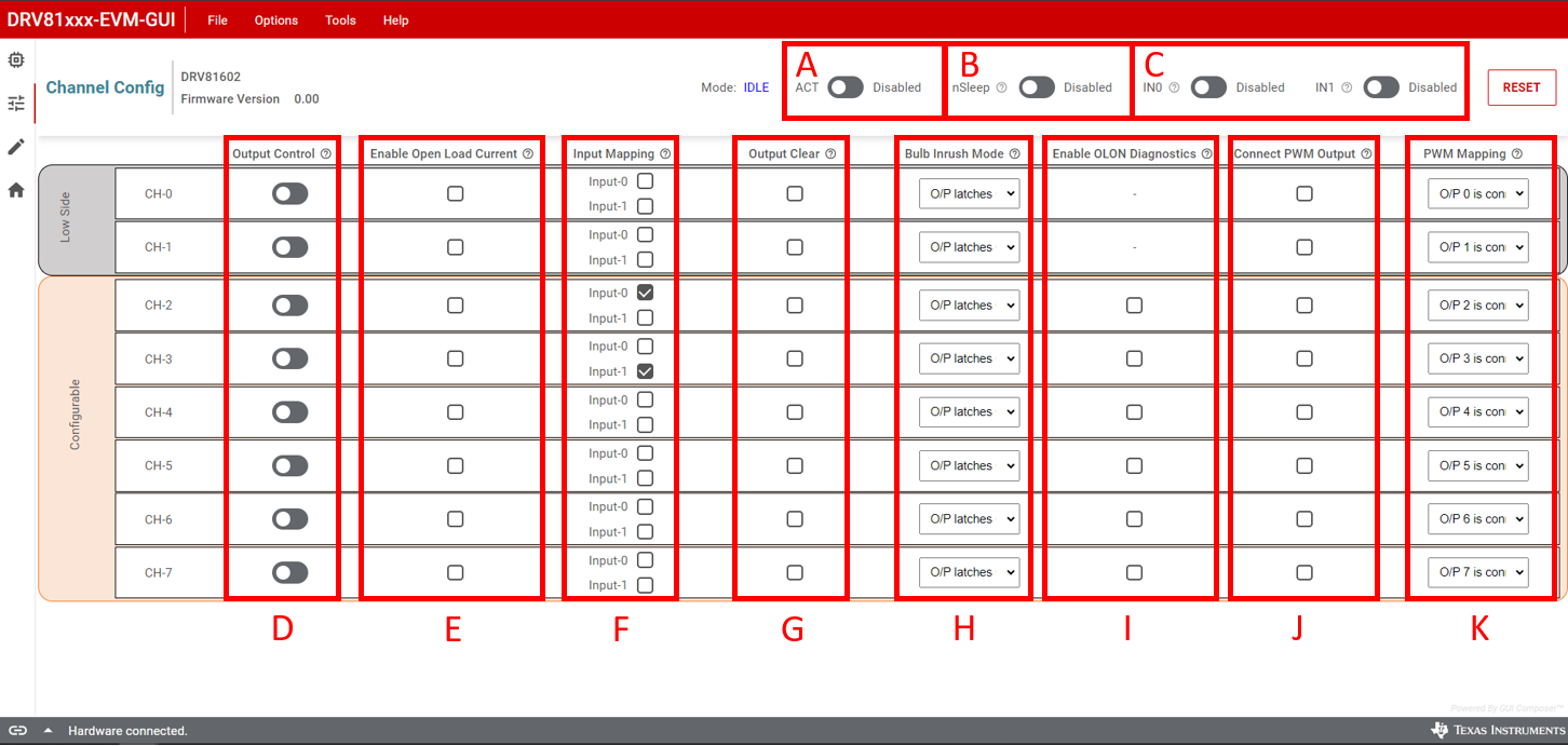
DRV81008-Q1EVM, DRV81602-Q1EVM, DRV81242-Q1EVM,  DRV81602-Q1 GUI Channel
                    Configuration Page Figure 3-9 DRV81602-Q1 GUI Channel Configuration Page
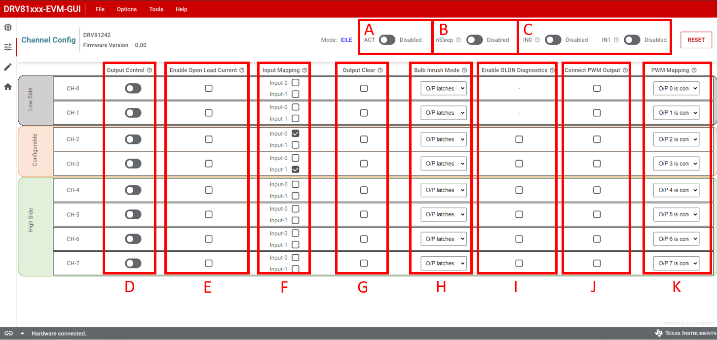
DRV81008-Q1EVM, DRV81602-Q1EVM, DRV81242-Q1EVM,  DRV81242-Q1 GUI Channel
                    Configuration Page Figure 3-10 DRV81242-Q1 GUI Channel Configuration Page
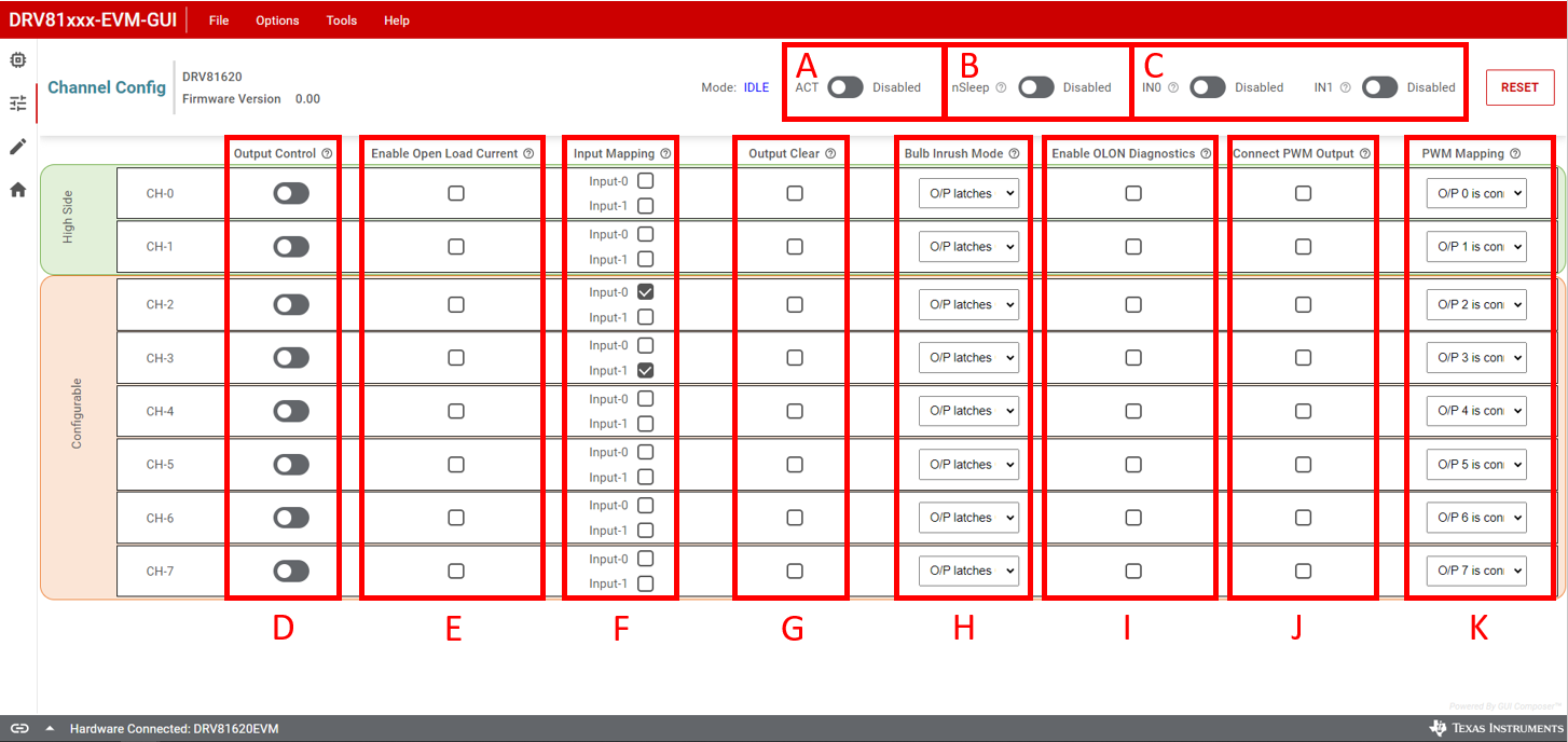
DRV81008-Q1EVM, DRV81602-Q1EVM, DRV81242-Q1EVM,  DRV81620-Q1 GUI Channel
                    Configuration Page Figure 3-11 DRV81620-Q1 GUI Channel Configuration Page
Table 3-3 DRV81602-Q1, DRV81242-Q1, and DRV81620-Q1
Component Description

A

Active Mode

  • Disabled (default): device in Idle Mode.
  • Enabled: device in Active Mode.

B

nSLEEP

  • Disabled (default): low-current sleep mode.
  • Enabled: activates Idle mode.

C

Input Pins (IN0 and IN1)

  • Disabled: the input pin is set to logic low.
  • Enabled: the input pin is set to logic high.

D

Output Control

  • Disabled (default): Output x is OFF.
  • Enabled: Output is ON.

E

Enable Open Load Current

  • Disabled (default): IOL current source not enabled.
  • Enabled: IOL current source enabled.

F

Input Mapping

  • Disabled (default): output x is not connected to the input pin..
  • Enabled: output x is connected to the input pin.
Note:

By default, IN0 is connected to CH-2 and IN1 is connected to CH-3.

G

Output Clear

  • Disabled (default): normal operation.
  • Enabled: clear the error latch for the selected output.

H

Bulb Inrush Mode

  • Disabled (default): Output latches OFF in case of errors.
  • Enabled: output restarts automatically in case of errors.

I

Enable OLON Diagnostics

  • Disabled (default): normal operation or diagnosis performed on channel OFF.
  • Enabled: open load at ON detected.

J

Connect PWM Output

  • Disabled (default): PWM generator not connected to output.
  • Enabled: PWM generator connected to output.

K

PWM Mapping

  • 0: output connected to PWM generator 0.
  • 1: output connected to PWM generator 1.