SLYA042 July 2024 FDC1004 , FDC1004-Q1
- 1
- Abstract
- Trademarks
- 1 Introduction
- 2 CSAs and Input Bias Stage
- 3 CSA and Gain Error Factor
- 4 Applications for Resistance at Input Pins of Current Sense Amplifiers
- 5 Applications for Input Resistance at Reference Pins of Current Sense Amplifiers
- 6 Design Procedure and Error Calculation for External Input Resistance on CSA
- 7 Design Procedure for Input Resistance on Capacitively-Coupled Current Sense Amplifier
- 8 Design Procedure for Input Resistance at CSA Reference Pins
- 9 Input Resistance Error Test with INA185 Over Temperature
- 10Input Resistance Error Test with INA191 Over Temperature
- 11Derivation of VOS, EXT for a Single Stage Current Sense Amplifier (CSA)
- 12Summary
- 13References
2 CSAs and Input Bias Stage
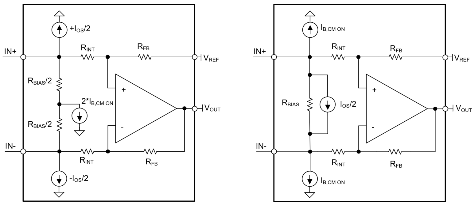
The input bias stage allows CSAs to operate with supply voltages (VS) independent of input common-mode voltage (VCM). For most devices, the input bias stage has a resistance (RBIAS) in between input pins ranging from 2kΩ to 72kΩ. This resistances creates an effective differential bias current (IB, Differential) that is proportional to the input differential shunt voltage.
 Figure 2-1 Simplified Equivalent Models
of Single Stage Current Sense Amplifier With Input Bias Stage
Figure 2-1 Simplified Equivalent Models
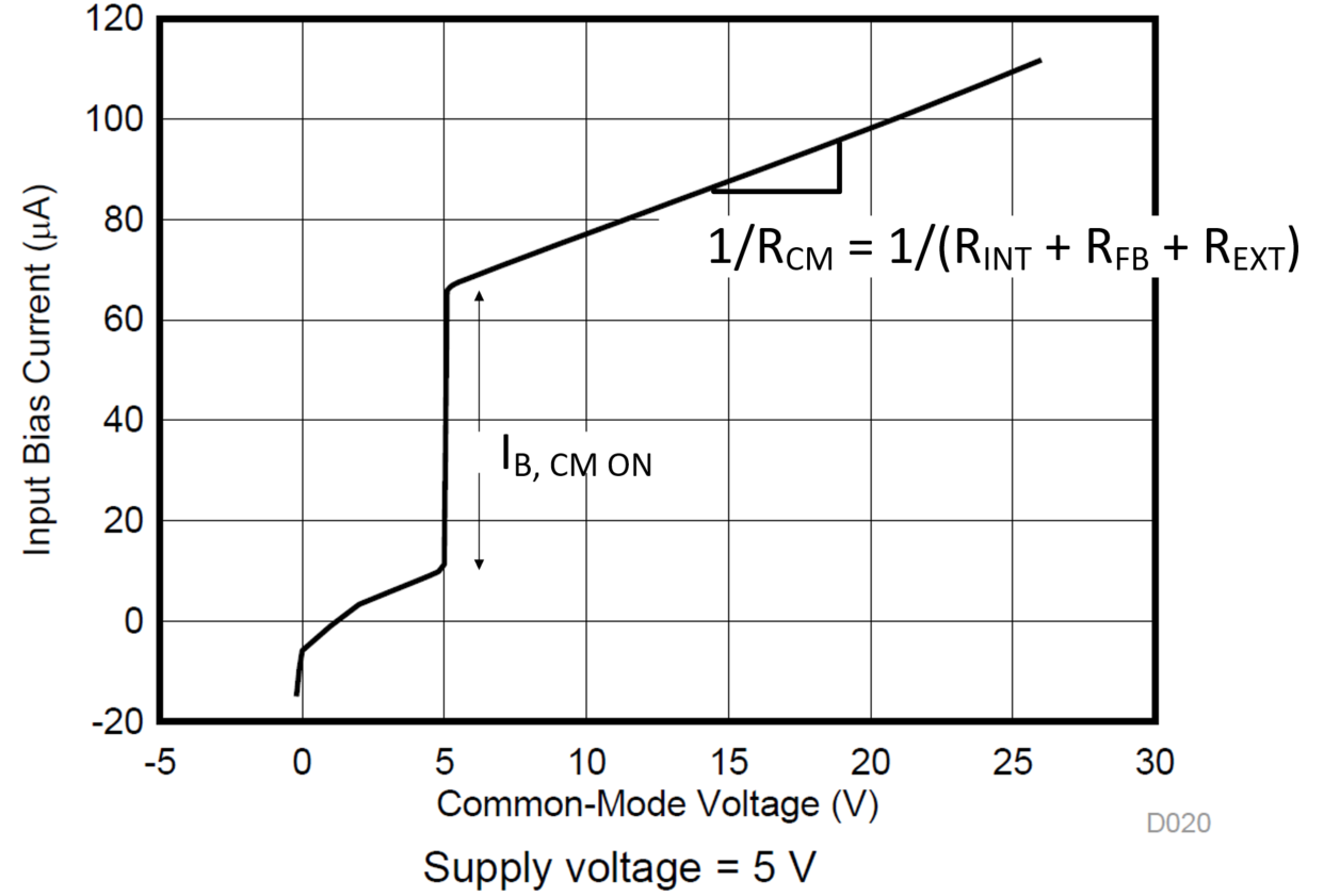
of Single Stage Current Sense Amplifier With Input Bias StageWithin the input bias stage is circuitry that monitors the VCM to appropriately turn on a bias current (IB, CM ON). This usually occurs when VCM exceeds VS or some proportional value (check data sheet). For example with the single-stage CSA, INA185, a large jump in total input bias current occurs when VCM exceeds the 5V supply voltage.
 Figure 2-2 Input Bias Current vs Input
Common-Mode Voltage for INA185
Figure 2-2 Input Bias Current vs Input
Common-Mode Voltage for INA185Aside from this shift, the total IB, CM is the general leakage current (IB, Leakage) from bus voltage at input pins to the reference voltage at REF pin. Thus the total input bias current for each input pin is the summation of common-mode leakage from bus to reference, IB, CM ON, and the differential current through RBIAS.
Note for two-stage CSAs, the IB, Leakage is determined by difference between VCM and the internal bias voltage (VCM2) in between first and second stage; however, please defer to the input bias current data plots in data sheets as current pathway can be more complex.
Understanding input bias currents is important as input bias determine offset error from external input resistance (VOS, EXT).