SLYT818 November 2021 LM74701-Q1 , LM74721-Q1
- 1 Introduction
- 2 Automotive reverse-battery protection with ideal diode controllers
- 3 TVS-less automotive reverse-polarity protection using ideal diode controllers
- 4 TVS-less ideal diode: mode of operation and working principle
- 5 External MOSFET
- 6 Output Capacitor (COUT)
- 7 TVS-less ideal diode controller EMC performance
- 8 Conclusion
- 9 Related Websites
- 10Important Notice
5 External MOSFET
Select an external MOSFET that achieves the best trade-off between power dissipation, system-level performance (such as reverse-current blocking) and solution cost. A MOSFET that typically provides 30 mV to 50 mV of forward drop at a full load current is a good starting point.
Another important parameter is the MOSFET’s maximum VDS voltage rating. During the ISO 7637-2 Pulse 1 transient event, the maximum VDS seen by the external MOSFET Q1 is the VDSCLAMP (max) detection threshold of an ideal diode controller. Equation 1 calculates the peak current flowing through the MOSFET during the ISO 7637-2 Pulse 1 transient event:
where:
VISO is the negative peak of ISO 7637-2 Pulse 1 transient event,
VOUT is the initial level of the VBATT before applying the ISO 7637-2 Pulse 1,
VDSCLAMP is the maximum VCLAMP threshold of the ideal diode controller and
RS is the ISO 7637-2 pulse-generator input impedance (10 Ω).
Figure 5-1 shows the LM74701-Q1’s TVS-less performance during ISO 7637-2 Pulse 1 transient event, along with gate turn on behavior during VDS clamp operation, peak pulse current and power dissipation across the MOSFET.
 Figure 5-1 LM74701-Q1 ideal diode
controller TVS-less performance.
Figure 5-1 LM74701-Q1 ideal diode
controller TVS-less performance.The average current during an ISO 7637-2 pulse can be approximated as one-third the peak current, or (IISO_PEAK/3). So Equation 2 calculates the average power dissipated across the external MOSFET:
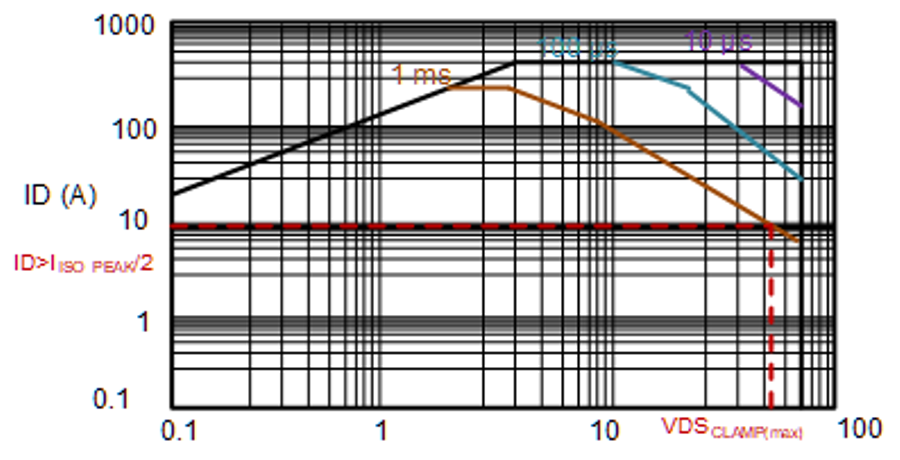
An ISO 7637-2 Pulse 1 transient event lasts for typically 2 ms, and the external MOSFET operates in active clamp mode for about 1 ms. Selecting a MOSFET with safe operating area (SoA) characteristics – with the load line corresponding to the VDS of VDSCLAMP (max) and drain current (ID) greater than (IISO_PEAK/2) for 1 ms is a suitable option.
Figure 5-2 shows typical SoA characteristics and example selection criteria for the MOSFET.
 Figure 5-2 Example MOSFET SoA selection
curve.