SNOAA61A October 2020 – February 2021 LMG3422R030 , LMG3422R050 , LMG3425R030 , LMG3425R050
4.1 Finite Element Models for Thermal Analysis
Simulation models were built using ANSYS finite element analysis (FEA) software in order to compare thermal performance (i.e., RθJC/P) of different surface-mount packages. Illustrations of four models including QFN 8x8, QFN 12x12, TOLL, and D2PAK packages are shown in Figure 4-1. The former two QFN packages are implemented for TI’s 600-V GaN power stage products while the latter two are used by competitors for their commercially released 600-V GaN and 650-V SiC discrete devices respectively. Each surface-mount device is placed on the center of a 4-layer PCB in 40-mm x 40-mm surface area and 1.58-mm thickness.
 Figure 4-1 Simulation Models Built for Different Packages:
(a) QFN 8x8, (b) QFN 12x12, (c) TOLL, and (d)
D2PAK
Figure 4-1 Simulation Models Built for Different Packages:
(a) QFN 8x8, (b) QFN 12x12, (c) TOLL, and (d)
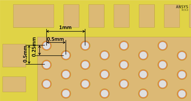
D2PAKAn example cross-sectional view of the generated model with a detailed description on the multilayer PCB structure is displayed in Figure 4-2. Most building elements including thermal via patten design (Figure 4-3) are the same for all built models except two items: PCB top Cu layer design and total numbers of thermal vias, which were adjusted to fit for the thermal pad area of each package for the purpose of a fair thermal performance comparison among different packages. Please note that the top Cu pad for heat spreading and the corresponding thermal via pattern/number can be further optimized for specific applications. Table 4-1 summarizes the key dimensional and thermal information for major modelling components.
 Figure 4-2 Cross-Section View of Simulation Model (QFN
8x8)
 Figure 4-3 Thermal Via Pattern on PCB
| COMPONENT | THICKNESS (mm) | MATERIAL | THERMAL CONDUCTIVITY (W/mK) |
|---|---|---|---|
| Solder | 0.05 | Lead-free solder | 50 |
| PCB | 0.12 (prepreg)/1.06 (core) | FR4 | 0.3 |
| 0.07 (4 layers) | Cu | 385 | |
| Thermal Via | 0.025 | Cu plating | 385 |
| 0.2 (diameter) | Epoxy via filling | 1 | |
| TIM | 1 | Gap filler pad | 8 |
| Coldplate | 2.5 | Aluminum alloy | 160 |