SSZT800 february 2018 TPS543B20 , TPS543C20
Previously, in my last blog "Powering FPGAs - Improving undershoot of voltage regulators with asynchronous pulse injection" we discussed how Asynchronous Pulse Injection (API) could reduce the undershoot of a fixed frequency DC/DC converter during a sudden increase in load current. Now I would like to discuss a feature that helps address the overshoot needs of the Arria 10, Stratix 10, or similar FPGAs. Overshoot reduction is critical for digital point of loads such as the Arria 10 and Stratix 10 devices because excessive supply voltage can stress or even damage sensitive, high-speed circuits.
First, let’s understand how fixed frequency DC/DC converters respond to a sudden decrease in load current in order to maintain the regulated output voltage. In order to limit the amount of rise in output voltage, the low-side field-effect transistor (FET) of the converter turns on in order to sink the voltage. During this time, the voltage across the inductor is very close to the actual output voltage. Equation 1 computes the voltage across the inductor with the low-side FET on:
where VLLS ON is the inductor voltage with the low-side FET on, VOUT is the output voltage, IL is the inductor current, DCR is the DC resistance of the inductor, Rtrace is the trace resistance of the printed circuit board (PCB) and RDS(on) is the drain-source resistance of the low-side FET.
Equation 2 defines the rate at which the current drops:
Equation 3 defines the total charge that the output capacitor must absorb during a load step down:
where ∆ILOAD is the load-transient step size.
Now consider what would happen if instead of turning the low-side FET on during a sudden load current decrease, you turned it off. This feature is known as overshoot reduction (OSR), or “body brake.” By turning off both the high- and low-side FETs during a rapid load current decrease, you can limit the amount of overshoot.
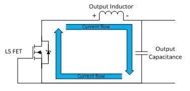
Let’s look at what happens to the flow of current when the low-side FET turns off and reevaluate Equation 1, which computed the voltage across the inductor. Figure 1 shows the current flow when the low-side FET is turned off, in which the current flows out of the inductor into the output capacitor, out of the output capacitor into ground, out of ground and through the body diode of the low-side FET, and back to the inductor.
 Figure 1 Current Flow During
OSR
Figure 1 Current Flow During
OSREquation 2 computed the voltage across the inductor with the low-side FET on. What happens to this equation when the low-side FET is off? RDS(on) is no longer a factor, but the forward voltage drop of the low-side FET body-diode is, as shown in Equation 4:
Since the voltage drop across the body diode of the low-side FET is greater than the conduction channel (IL x Rdson), you can see that:
Therefore, VLLS_OFF results in a larger, negative voltage across the inductor. This larger negative voltage causes the inductor current to slew down faster, resulting in less total charge flowing into the output capacitor (replacing VLLS_ON with VLLS_OFF in Equation 3) and producing less overshoot.
Now let’s look at a simulation of a model with and without OSR enabled. Table 1 shows a common rail voltage rating for Arria 10 field-programmable gate arrays (FPGAs).
| Min | Typ | Max | Unit |
|---|---|---|---|
| 0.92 | 0.95 | 0.98 | V |
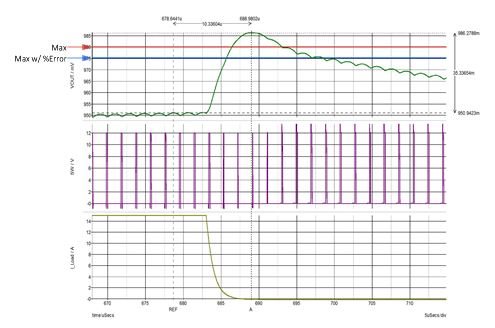
Figure 2 shows a load-transient simulation of a fixed-frequency converter without OSR. The load current, or the lower waveform in Figure 2, steps down. As a result, the output voltage, or the upper waveform in Figure 2, rises above the required maximum operating voltage labeled “max” at 0.98V.
In addition to the required maximum and minimum values for this particular rail, there is a percentage of error associated with the actual output voltage of the power supply when compared to the target voltage. Two devices that offer OSR, the TPS543B20 and TPS543C20 from Texas Instruments, have an adjustable reference voltage with 0.5% accuracy that you can set to the target output voltage of 0.95V. This means that you can improve the percentage of output voltage accuracy error by removing the deviation caused by the tolerance of the feedback resistor divider. The resulting output voltage accuracy error percentage is approximately ±0.5%. This decreases the amount of available tolerance by ±4.75mV, which is also shown in Figure 2, labeled “Max w/ %Error” at 975mV.
 Figure 2 A Load-transient Simulation of
a Fixed-frequency Converter with OSR Disabled
Figure 2 A Load-transient Simulation of
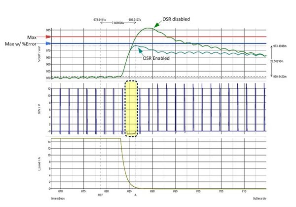
a Fixed-frequency Converter with OSR DisabledFigure 3 shows a load-transient simulation of a fixed-frequency converter with OSR enabled. The upper waveform in Figure 3 is the output voltage, which now remains within the operating range of the expected voltage values listed in Table 1 labeled “Min,” as well as the minimum when accounting for output voltage accuracy labeled “Min w/ %Error” at 975mV. The middle waveform in Figure 3 is the switch node; you can see that the load current, or the lower waveform in Figure 3, steps down at the same point with respect to the switching cycle compared to the previous simulation. The difference is that both the high- and low-side FETs are off, as indicated by the highlighted portion of the switch node.
 Figure 3 A Load-transient Simulation of
a Fixed-frequency Converter with OSR Enabled
Figure 3 A Load-transient Simulation of
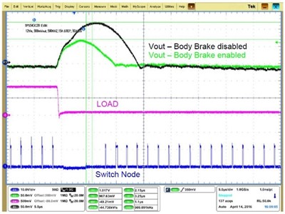
a Fixed-frequency Converter with OSR EnabledFigure 4 shows the difference with OSR (body brake) enabled and disabled on actual bench results of the TPS543C20. The test configuration was a 12V input voltage, 0.9V output voltage, 500kHz switching frequency and 15A step up/step down with a slew rate of 50A/µs. When comparing the same device with and without this feature enabled, the overshoot was approximately 49mV less with OSR enabled.
 Figure 4 Overshoot with OSR
Enabled/disabled
Figure 4 Overshoot with OSR
Enabled/disabledTable 2 lists two devices currently available with OSR and asynchronous pulse injection (API) used to limit undershoot, as well as a few key features for these devices. These devices offer API adjustability and the ability to enable or disable API and OSR.
| TPS543B20 | TPS543C20 | |
|---|---|---|
| API | Yes | Yes |
| OSR | Yes | Yes |
| High-side FET RDS(on) | 4.1mΩ | 3mΩ |
| Low-side FET RDS(on) | 1.9mΩ | 0.9mΩ |
| Current rating | 25A | 40A-80A* |
| Comments | *Device is stackable up to two phases |
Using Texas Instruments devices with the features listed here showed improvement in regards to the total amount of undershoot and overshoot when compared to having these features disabled. With these features, you can meet voltage regulation requirements with less output capacitance, which is something to consider when designing in Stratix 10 and Arria FPGAs.
Additional Resources
- Get more information on powering the Arria 10 and Stratix 10 FPGAs.
- Estimate actual load current and transient specifications for Altera devices with the Early Power Estimator (EPE) and Power Delivery Network (PDN).
- Learn more about TI power management for Altera FPGAs.