-
Benefits Using a Buck Converter's External Vcc Bias Pin
Benefits Using a Buck Converter's External Vcc Bias Pin
Trademarks
All trademarks are the property of their respective owners.
1 DC/DC Converters with Internal LDO
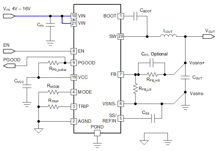
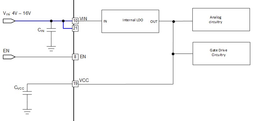
The input voltage of a DC/DC step-down converter is internally routed to analog circuitry, gate-drive circuitry, and the drain of the high-side MOSFET for power conversion. Since it is impractical and unnecessary to use a higher voltage semiconductor process for analog and gate-drive circuits, a separate internal LDO regulator is integrated into the DC/DC converter to provide power to these circuits. Figure 1-1 illustrates a typical DC/DC converter accepting a 4-V to 16-V input onto the VIN pins and Figure 1-2 shows an internal LDO providing power to the analog and gate-drive circuitry. The internal LDO powers all the analog circuitry and logic inside the IC, and its voltage may optimized for different voltage levels needed by the circuitry. The internal LDO steps-down the VIN voltage to the VCC voltage and the voltage-drop across the LDO causes power to be dissipated in the LDO. Since the load of the internal LDO is IVCC, the power dissipated by the internal LDO is (VIN – VLDO)*IVCC. A larger bias current and higher voltage-drop causes the DC/DC converter's efficiency to decrease.
 Figure 1-1 Typical DC/DC Converter with
Single Input Voltage
 Figure 1-2 DC/DC Converter with
Integrated Internal LDO
Figure 1-2 DC/DC Converter with
Integrated Internal LDO2 DC/DC Converters with External Bias
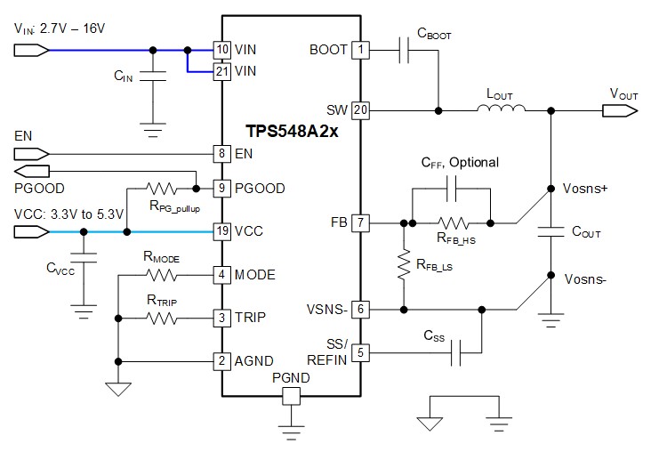
Several DC/DC converters on the market have an additional pin that accepts an externally applied voltage, such as the TPS548A28 and TPS548A29 shown in Table 2-1. An external bias voltage, also called a split-bias rail voltage, above the internal LDO's output voltage will override the internal LDO and enhance the efficiency of the converter by eliminating its power loss. The VCC current will be supplied from the external bias instead of the internal LDO. Figure 2-1 shows an external bias voltage applied to the VCC pin allowing a lower input voltage into the VIN pins. The VCC pin needs to be bypassed with a 2.2 μF ceramic capacitor, CVCC with a 6.3-V or higher rating as shown in Figure 1-1 and Figure 2-1. The external VCC voltage is supplied by a separate DC/DC converter or connected directly from an existing 3.3-V or 5-V voltage source already available on the circuit board.
| Device | Output Current | Internal LDO Voltage | External Bias Voltage Range | Power Stage Voltage Range with External Bias Voltage | Power Stage Voltage Range with Internal LDO Voltage |
|---|---|---|---|---|---|
| TPS548A28 | 15-A | 3-V | 3.13-V to 5.3-V | 2.7-V to 16-V | 4-V to 16-V |
| TPS548A29 | 15-A | 4.5-V | 4.75-V to 5.3-V | 2.7-V to 16V | 4-V to 16-V |
 Figure 2-1 Typical DC/DC Converter with Split-Bias Rail Input Voltages
3 Efficiency and Power Loss Calculations
The power efficiency formula is shown in Equation 1 and the power loss formula is shown in Equation 2. Power loss results in Watts are easier to compare than efficiency numbers, especially in multi-rail systems because a watt is more specific than an efficiency percentage when considering power dissipation.
Equation 3 and Equation 4 show the power losses of the internal LDO and demonstrate that additional losses are present depending on the efficiency of the internal LDO, using 25% efficiency as an example.
When the VCC pin is connected to an external source that is greater than the internal LDO output voltage, the internal LDO is turned off, power is drawn from the external source, and the internal LDO power loss (VIN-VLDO)*IVCC is zero resulting in increased efficiency of the converter. However, if the IBIAS current is provided by an additional DC/DC converter, its own power losses need to be considered into the total system efficiency. If the additional DC/DC converter is a synchronous buck converter, the power losses will be lower than the internal LDO power losses. The internal LDO also provides the voltage for boot capacitor CBOOT to provide the gate-drive voltage to drive the power MOSFETs. When the external VCC is higher than the internal LDO voltage, the gate-drive voltage increases, lowering the RDS(on) of the MOSFETs and increasing the efficiency, especially at higher output current.