DLPU100B May 2020 – June 2024 DLP2021-Q1 , DLP3021-Q1
- 1
- Abstract
- Trademarks
- 1Introduction
- 2FPGA Pin Configuration and Functions
- 3Specifications
- 4Feature Descriptions
- 5Layout
- 6Host Command Protocol
- 7FPGA Register Definitions
- 8Revision History
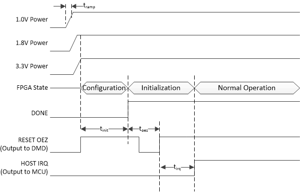
3.4.1 Power-Up Timing
Table 3-4 specifies the configuration and initialization timing during FPGA start-up. After Host_irq gets set high, the FPGA is configured and ready to receive commands on the SPI interface. However, the first commands will not be executed for an additional 10 ms.
Table 3-4 Power-up Timing
Specifications
| MIN | NOM | MAX | UNIT | ||
|---|---|---|---|---|---|
| tinit(2) | FPGA configuration initialization. 1.8V power to DONE rising edge | 230 | ms | ||
| toez | DONE rising edge to DMD RESET OEZ low | 8.5 | ms | ||
| tirq(3) | RESET OEZ low to HOST IRQ high | 1.15 | ms | ||
| tramp(1) | Ramp time for each power supply: 1.0V, 1.8V, and 3.3V (GND to 90% reference points) | 0.2 | 50 | ms |
(1) Value is based on FPGA documentation available at the time of
writing. As primary source specification, see the device-specific FPGA data
sheet.
(2) INITZ should be pulled up to 1.8V for shortest start-up time.
If INITZ rising edge is delayed then the configuration will be delayed.
(3) HOST IRQ ready bit will indicate that the FPGA is ready for SPI
communication from a host. This bit must be set in the interrupt enable mask in
order for this condition to set HOST IRQ high at startup. The interrupt enable
mask can be automatically configured on startup from the default
configuration.
 Figure 3-2 Power-up Timing
Diagram