DLPU100B May   2020  – June 2024 DLP2021-Q1 , DLP3021-Q1


  1.   1
  2.   Abstract
  3.   Trademarks
  4. 1Introduction
    1. 1.1 Purpose and Scope
  5. 2FPGA Pin Configuration and Functions
    1. 2.1 DMD Interface
    2. 2.2 Light Control
    3. 2.3 Communication
    4. 2.4 Support
    5. 2.5 FPGA Dedicated Pins
    6. 2.6 Power and Ground
    7. 2.7 Unused Pins
  6. 3Specifications
    1. 3.1 Recommended Operating Conditions
    2. 3.2 FPGA Power Consumption
    3. 3.3 Host SPI Interface Timing
    4. 3.4 Power Supply and Reset Timing
      1. 3.4.1 Power-Up Timing
      2. 3.4.2 Power-Down Timing
      3. 3.4.3 Brownout Detection
    5. 3.5 DMD Interface Timing
    6. 3.6 Flash Memory Interface Timing
    7. 3.7 Reference Clock Timing
    8. 3.8 I2C Interface Timing
  7. 4Feature Descriptions
    1. 4.1 Video Control
      1. 4.1.1 Video Options
      2. 4.1.2 Example 1: Display a Static Image
      3. 4.1.3 Example 2: Display 1 Video Repeatedly
      4. 4.1.4 Example 3: Display Two Videos Then Stop
      5. 4.1.5 Example 4: Display a Video Once and Then Display an Image Forever
      6. 4.1.6 Example 5: Display 3+ Videos/Images Seamlessly
    2. 4.2 Temperature Measurements
    3. 4.3 PWM Outputs
    4. 4.4 Host IRQ Interrupt Signal
    5. 4.5 Video and Image Compression
  8. 5Layout
  9. 6Host Command Protocol
    1. 6.1 SPI Specifications
    2. 6.2 SPI Write Command
    3. 6.3 SPI Read Command
  10. 7FPGA Register Definitions
  11. 8Revision History

Power-Down Timing

Table 3-5 Power-Down Timing Specifications
MIN NOM MAX UNIT
tpark Time required for DMD to properly park(1)(2) 500 µs
tdebounce Time required for input voltage to remain below brownout detection threshold before park sequence begins. 100 µs
DMD voltages (2.5V, 1.8V, 8.5V, 16V, –10V) must remain valid until parked on DLP3021-Q1
DMD voltages (1.8V, 8.5V, 16V, –10V) must remain valid until parked on DLP2021-Q1
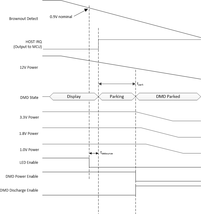
DLP3021-Q1 Power-Down Timing
                    Diagram Figure 3-3 Power-Down Timing Diagram