DLPU100B May   2020  – June 2024 DLP2021-Q1 , DLP3021-Q1


  1.   1
  2.   Abstract
  3.   Trademarks
  4. 1Introduction
    1. 1.1 Purpose and Scope
  5. 2FPGA Pin Configuration and Functions
    1. 2.1 DMD Interface
    2. 2.2 Light Control
    3. 2.3 Communication
    4. 2.4 Support
    5. 2.5 FPGA Dedicated Pins
    6. 2.6 Power and Ground
    7. 2.7 Unused Pins
  6. 3Specifications
    1. 3.1 Recommended Operating Conditions
    2. 3.2 FPGA Power Consumption
    3. 3.3 Host SPI Interface Timing
    4. 3.4 Power Supply and Reset Timing
      1. 3.4.1 Power-Up Timing
      2. 3.4.2 Power-Down Timing
      3. 3.4.3 Brownout Detection
    5. 3.5 DMD Interface Timing
    6. 3.6 Flash Memory Interface Timing
    7. 3.7 Reference Clock Timing
    8. 3.8 I2C Interface Timing
  7. 4Feature Descriptions
    1. 4.1 Video Control
      1. 4.1.1 Video Options
      2. 4.1.2 Example 1: Display a Static Image
      3. 4.1.3 Example 2: Display 1 Video Repeatedly
      4. 4.1.4 Example 3: Display Two Videos Then Stop
      5. 4.1.5 Example 4: Display a Video Once and Then Display an Image Forever
      6. 4.1.6 Example 5: Display 3+ Videos/Images Seamlessly
    2. 4.2 Temperature Measurements
    3. 4.3 PWM Outputs
    4. 4.4 Host IRQ Interrupt Signal
    5. 4.5 Video and Image Compression
  8. 5Layout
  9. 6Host Command Protocol
    1. 6.1 SPI Specifications
    2. 6.2 SPI Write Command
    3. 6.3 SPI Read Command
  10. 7FPGA Register Definitions
  11. 8Revision History

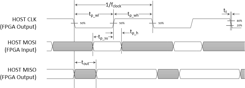
Host SPI Interface Timing

Table 3-3 Host SPI Interface Timing
Description MIN MAX UNIT
fclock Clock frequency, HOST CLK

(50% reference points)

5 MHz
tsu Setup time – HOST MOSI valid before HOST CLK capture edge

(50% reference points)

0 ns
th Hold time – HOST MOSI valid before HOST CLK capture edge

(50% reference points)

20 ns
tout Clock to data out – HOST MISO from HOST CLK transition edge

(50% reference points)

40 60 ns
DLP3021-Q1 Host SPI Interface Timing
                    Diagram Figure 3-1 Host SPI Interface Timing Diagram