DLPU100B May   2020  – June 2024 DLP2021-Q1 , DLP3021-Q1


  1.   1
  2.   Abstract
  3.   Trademarks
  4. 1Introduction
    1. 1.1 Purpose and Scope
  5. 2FPGA Pin Configuration and Functions
    1. 2.1 DMD Interface
    2. 2.2 Light Control
    3. 2.3 Communication
    4. 2.4 Support
    5. 2.5 FPGA Dedicated Pins
    6. 2.6 Power and Ground
    7. 2.7 Unused Pins
  6. 3Specifications
    1. 3.1 Recommended Operating Conditions
    2. 3.2 FPGA Power Consumption
    3. 3.3 Host SPI Interface Timing
    4. 3.4 Power Supply and Reset Timing
      1. 3.4.1 Power-Up Timing
      2. 3.4.2 Power-Down Timing
      3. 3.4.3 Brownout Detection
    5. 3.5 DMD Interface Timing
    6. 3.6 Flash Memory Interface Timing
    7. 3.7 Reference Clock Timing
    8. 3.8 I2C Interface Timing
  7. 4Feature Descriptions
    1. 4.1 Video Control
      1. 4.1.1 Video Options
      2. 4.1.2 Example 1: Display a Static Image
      3. 4.1.3 Example 2: Display 1 Video Repeatedly
      4. 4.1.4 Example 3: Display Two Videos Then Stop
      5. 4.1.5 Example 4: Display a Video Once and Then Display an Image Forever
      6. 4.1.6 Example 5: Display 3+ Videos/Images Seamlessly
    2. 4.2 Temperature Measurements
    3. 4.3 PWM Outputs
    4. 4.4 Host IRQ Interrupt Signal
    5. 4.5 Video and Image Compression
  8. 5Layout
  9. 6Host Command Protocol
    1. 6.1 SPI Specifications
    2. 6.2 SPI Write Command
    3. 6.3 SPI Read Command
  10. 7FPGA Register Definitions
  11. 8Revision History

Purpose and Scope

In this application, the FPGA reads video data directly from a Flash memory to display on the DMD. The FPGA also coordinates the illumination timing to coordinate with the displayed video content.
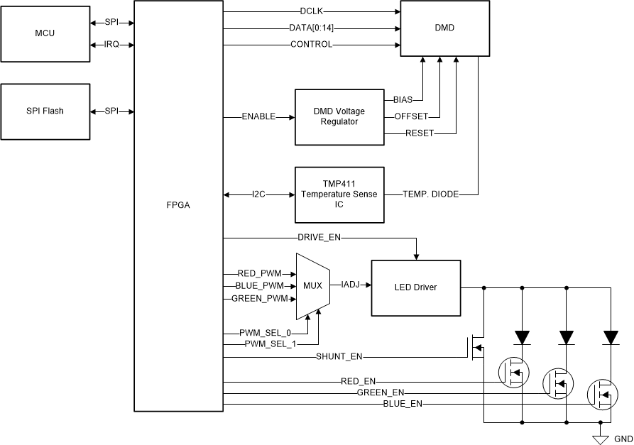
DLP3021-Q1 Dynamic Ground Projection
                    Electronics Block Diagram Figure 1-1 Dynamic Ground Projection Electronics Block Diagram