DLPU133A March 2024 – February 2025 DLPC964
- 1
- Abstract
- Trademarks
- 1Overview
-
2Apps FPGA
Modules
- 3.1 Apps FPGA Block Diagram
- 3.2 BPG Module
- 3.3 BRG Module
- 3.4 BRG_ST Module
- 3.5 PGEN Module
- 3.6 PGEN_MCTRL Module
- 3.7 PGEN_SCTRL Module
- 3.8 PGEN_PRM Module
- 3.9 PGEN_ADDR_ROM
- 3.10 HSSTOP Module
- 3.11 SSF Module
- 3.12 ENC Module
- 3.13 Xilinx IP
- 3.14 Reference Documents
- 3.15 DLPC964 Apps FPGA IO
- 3.16 Key Definitions
- 3Functional Configuration
-
4Appendix
- 5.1 Vivado Chipscope Captures
- 5.2 DLPC964 Apps Bitstream Loading
- 5.3
Interfacing To DLPC964 Controller with Aurora
64B/66B
- 5.3.1 Theory of Operation
- 5.3.2 Overview
- 5.3.3
Aurora 64B/66B TX Core and RTL Generation
- 5.3.3.1 Select Aurora 64B66B From IP Catalog
- 5.3.3.2 Configure Core Options
- 5.3.3.3 Lane Configurations
- 5.3.3.4 Shared Logic Options
- 5.3.3.5 Generate Example Design Files
- 5.3.3.6 RTL File List
- 5.3.3.7 Single Channel 3 Lanes Aurora Core RTL Wrapper
- 5.3.3.8 Four Channels 12 Lanes Top Level RTL Wrapper
- 5.3.3.9 Block Start with Block Control Word
- 5.3.3.10 Block Complete with DMDLOAD_REQ
- 5.3.3.11 DMDLOAD_REQ Setup Time Requirement
- 5.3.3.12 Single Channel Transfer Mode
- 5.3.3.13 DMD Block Array Data Mapping
- 5.3.3.14 Xilinx IBERT
- 5Abbreviations and Acronyms
- 6Related Documentation from Texas Instruments
- 7Revision History
4.3.3.12 Single Channel Transfer Mode
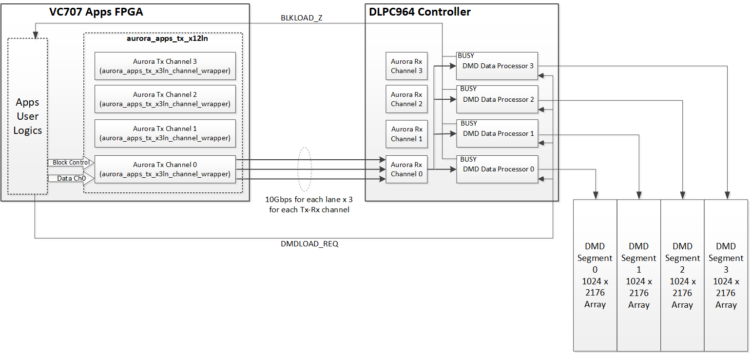
For non-critical pattern rate application, the DLPC964 supports operating with only Aurora channel 0. Only the three 10Gbps serial links for channel 0 are used and must be channel 0 in this mode of operation.
 Figure 4-23 System Block Diagram For Single Channel Operation
Operation is enabled by setting Block Control word field, SINGLE_CHANNEL = ‘1’ (Table 4-2 ), and transfer DMD segment in order of 3(first), 2, 1, 0(last) (DMD_SEGMENT field in Table 4-2 ). In other words, to control a particular DMD block, theApps FPGA must operate segment 3 of that block first, follow by segment 2, segment 1, and 0 being the last transfer segment.
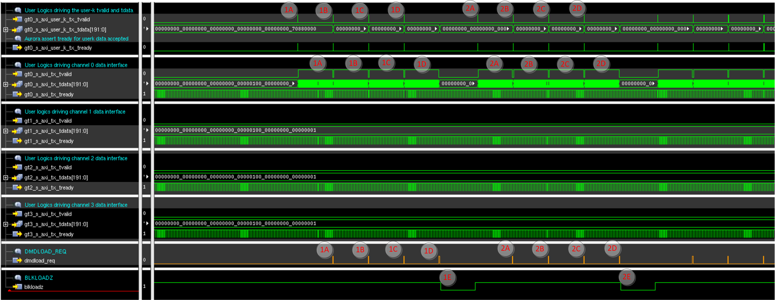
The guidelines stated in Section 4.3.3.9, Section 4.3.3.10, and Section 4.3.3.11, still apply to single channel operation mode where each block and segment Aurora transfer must still begin with a Block Control word and end with the DMDLOAD_REQ along with the 300ns setup time. However, one major difference regarding the Apps FPGA/DLPC964 handshaking in this mode is that the actual DMD operation only triggered by the DMDLOAD_REQ corresponds to segment 0; for example, BLKLOADZ is not asserted for segment 3, 2 and 1. (See Figure 4-24 for details).
All four segments of the selected block must be operated and in order of segment 3 (first), 2, 1 and 0 (last), otherwise the DLPC964 do not carry out the proper DMD operation to that block.
 Figure 4-24 Single Channel Operation Waveform Example
- Apps FPGA Aurora Data Transfer
for DMD Block 0 in Single Channel Mode.
- Block Control word, DMD data, and DMDLOAD_REQ for DMD block 0 Segment 3
- Block Control word, DMD data, and DMDLOAD_REQ for DMD block 0 Segment 2.
- Block Control word, DMD data, and DMDLOAD_REQ for DMD block 0 Segment 1.
- Block Control word, DMD data, and DMDLOAD_REQ for DMD block 0 Segment 0.
- Segment 0’s DMDLOAD_REQ triggers DLPC964 to begin block 0 data loading, assert BLKLOADZ to indicate operation in process.
- Apps FPGA Aurora Data Transfer
for DMD Block 1 in Single Channel Mode.
- Block Control word, DMD data, and DMDLOAD_REQ for DMD block 1 Segment 3.
- Block Control word, DMD data, and DMDLOAD_REQ for DMD block 1 Segment 2.
- Block Control word, DMD data, and DMDLOAD_REQ for DMD block 1 Segment 1.
- Block Control word, DMD data, and DMDLOAD_REQ for DMD block 1 Segment 0.
- Segment 0’s DMDLOAD_REQ triggers DLPC964 to begin block 1 data loading, assert BLKLOADZ to indicate operation in process.
Note that there is no data transfer happening on GT channel 1, 2, and 3. Only channel 0 is operated in this Single Channel mode.