SBAA532A February 2022 – March 2024 ADS1119 , ADS1120 , ADS1120-Q1 , ADS112C04 , ADS112U04 , ADS1130 , ADS1131 , ADS114S06 , ADS114S06B , ADS114S08 , ADS114S08B , ADS1158 , ADS1219 , ADS1220 , ADS122C04 , ADS122U04 , ADS1230 , ADS1231 , ADS1232 , ADS1234 , ADS1235 , ADS1235-Q1 , ADS124S06 , ADS124S08 , ADS1250 , ADS1251 , ADS1252 , ADS1253 , ADS1254 , ADS1255 , ADS1256 , ADS1257 , ADS1258 , ADS1258-EP , ADS1259 , ADS1259-Q1 , ADS125H01 , ADS125H02 , ADS1260 , ADS1260-Q1 , ADS1261 , ADS1261-Q1 , ADS1262 , ADS1263 , ADS127L01 , ADS130E08 , ADS131A02 , ADS131A04 , ADS131E04 , ADS131E06 , ADS131E08 , ADS131E08S , ADS131M02 , ADS131M03 , ADS131M04 , ADS131M06 , ADS131M08
- 1
- Abstract
- Trademarks
- 1Bridge Overview
- 2Bridge Construction
- 3Bridge Connections
- 4Electrical Characteristics of Bridge Measurements
- 5Signal Chain Design Considerations
-
6Bridge Measurement Circuits
- 6.1 Four-Wire Resistive Bridge Measurement with a Ratiometric Reference and a Unipolar, Low-Voltage (≤5 V) Excitation Source
- 6.2 Six-Wire Resistive Bridge Measurement With a Ratiometric Reference and a Unipolar, Low-Voltage (≤ 5 V) Excitation Source
- 6.3 Four-Wire Resistive Bridge Measurement With a Pseudo-Ratiometric Reference and a Unipolar, High-Voltage (> 5 V) Excitation Source
- 6.4 Four-Wire Resistive Bridge Measurement with a Pseudo-Ratiometric Reference and Asymmetric, High-Voltage (> 5 V) Excitation Source
- 6.5 Four-Wire Resistive Bridge Measurement With a Ratiometric Reference and Current Excitation
- 6.6 Measuring Multiple Four-Wire Resistive Bridges in Series with a Pseudo-Ratiometric Reference and a Unipolar, Low-Voltage (≤5V) Excitation Source
- 6.7 Measuring Multiple Four-Wire Resistive Bridges in Parallel Using a Single-Channel ADC With a Ratiometric Reference and a Unipolar, Low-Voltage (≤ 5 V) Excitation Source
- 6.8 Measuring Multiple Four-Wire Resistive Bridges in Parallel Using a Multichannel ADC With a Ratiometric Reference and a Unipolar, Low-Voltage (≤ 5 V) Excitation Source
- 7Summary
- 8Revision History
5.1.1.1 INA Architecture and Operation
Although there are other topologies, a basic three op-amp INA is shown in Figure 5-1.
 Figure 5-1 Topology of a Basic
INA
Figure 5-1 Topology of a Basic
INAThe INA in Figure 5-1 amplifies the voltage between AINP and AINN. The amplifier gain is determined by an external gain-setting resistor, RG, and the internal feedback resistors, RF. The voltages at AINP and AINN are forced onto RG via the output of A1 and A2 and both RF resistors. This forces the same current through all three resistors to create gain. A difference amplifier comprised of op amp A3 and four resistors, R, act as a unity gain buffer. The amplified voltage is measured between the REF and VOUT pins on the INA. The REF pin sets the reference point of the output voltage, and is typically chosen to match the ADC common-mode range. The INA gain is set by RG and is determined by Equation 18:
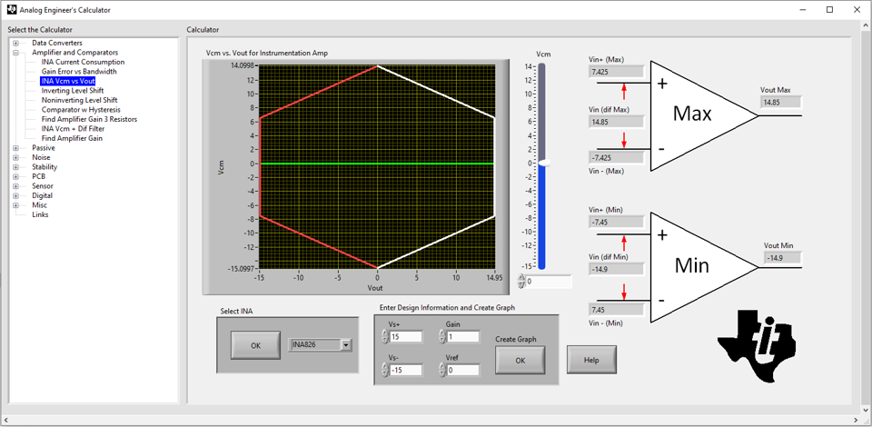
Most INAs are capable of large voltage gains up to 1000 V/V. However, one practical challenge associated with high gain is that it limits the input signal common-mode voltage to approximately mid-supply. In the INA topology, the input common-mode voltage must match the output common-mode of the first op amp stage comprised of A1 and A2 in Figure 5-1. As the voltage of RG is amplified to the output of A1 and A2, the output voltages of A1 and A2 are limited by how close those voltages are to either supply (V+ or V–). This limitation requires choosing the INA and bridge excitation supplies such that the bridge output is in the INA measurement range. The INA Vcm vs Vout tool in the Analog Engineer’s Calculator simplifies this process by calculating the input common-mode range against the output voltage for a range of INAs. Figure 5-2 shows an example of this tool using the INA826.
 Figure 5-2 INA Vcm vs Vout Tool in
the Analog Engineer's Calculator