SBAU412A November 2022 – May 2024 AFE7900 , AFE7903 , AFE7906 , AFE7920 , AFE7921 , AFE7950
- 1
- Abstract
- Trademarks
- 1 Introduction
- 2 Prerequisites
- 3 Typical Bare-Metal Design Flow
- 4 Background
- 5 Add Microblaze and SPI IP for Use in Vitis for Embedded Development
- 6 Create New Platforms in Vitis
- 7 Create New Application Projects in Vitis
- 8 Build Application Projects
- 9 Generate SPI Log for AFE79xx EVM
- 10AFE79xxEVM Board Modifications
- 11Configure the AXI GPIO
- 12Configure the AXI SPI
- 13Set Up and Power on Hardware
- 14Set up ZCU102 Board Interface for VADJ_FMC
- 15Debug Application Projects and Set up Vitis Serial Terminal
- 16Execute the Application
- 17Revision History
4 Background
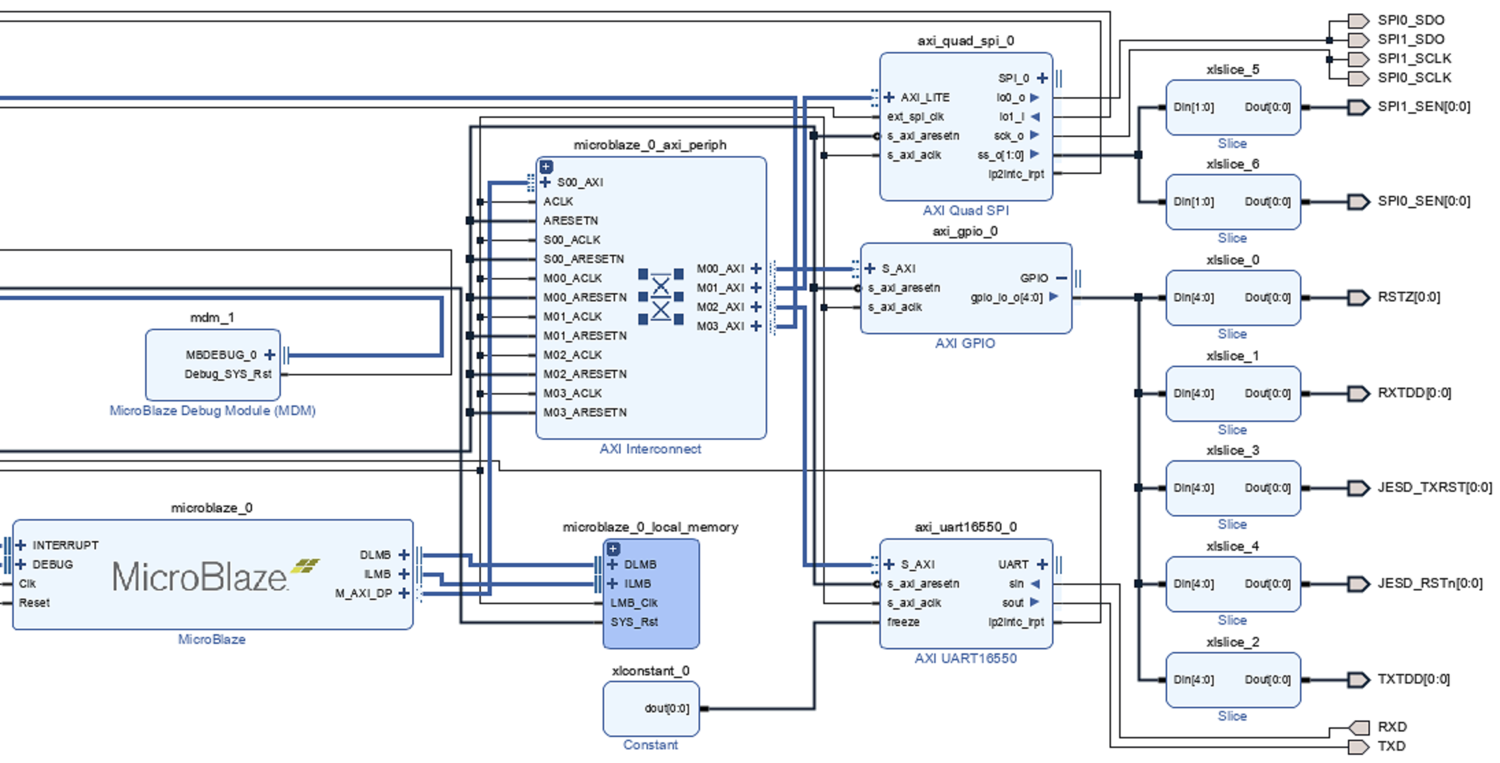
This example uses a soft core Microblaze because the Microblaze can be instantiated in most of the Xilinx FPGA families. The SPI, UART, and GPIO AXI blocks run on relatively lower frequency AXI clocks. As seen in Figure 4-1, the AXI peripherals are controlled by a Microblaze block through smart interconnects.
 Figure 4-1 Typical Block Design With
Microblaze and AXI Peripherals
Figure 4-1 Typical Block Design With
Microblaze and AXI PeripheralsThe HP port of the Microblaze drives AXI peripherals block design. The clocking of the entire IP is expected from a 100MHz differential clock source. This example uses a 100MHz differential clock source because this clock is typically available as ‘user clock’ in most FPGA EVMs. All other clock frequencies are derived internally through a clocking wizard. Depending on the number of independent SPI buses required in the system, more AXI SPI IPs can be added to the block design.