SBOS473L March   2009  – July 2024 TMP112 , TMP112D

PRODUCTION DATA  

  1.   1
  2. Features
  3. Applications
  4. Description
  5. Device Comparison
  6. Pin Configuration and Functions
  7. Specifications
    1. 6.1 Absolute Maximum Ratings
    2. 6.2 ESD Ratings
    3. 6.3 Recommended Operating Conditions
    4. 6.4 Thermal Information
    5. 6.5 Electrical Characteristics
    6. 6.6 Timing Requirements
    7. 6.7 Timing Diagrams
    8. 6.8 Typical Characteristics (TMP112A/B/N)
    9. 6.9 Typical Characteristics (TMP112Dx)
  8. Detailed Description
    1. 7.1 Overview
    2. 7.2 Functional Block Diagrams
    3. 7.3 Feature Description
      1. 7.3.1 Digital Temperature Output
      2. 7.3.2 Serial Interface
        1. 7.3.2.1 Bus Overview
        2. 7.3.2.2 Serial Bus Address
        3. 7.3.2.3 Writing and Reading Operation
        4. 7.3.2.4 Target Mode Operations
          1. 7.3.2.4.1 Target Receiver Mode
          2. 7.3.2.4.2 Target Transmitter Mode
        5. 7.3.2.5 SMBus Alert Function
        6. 7.3.2.6 General Call
        7. 7.3.2.7 High-Speed (Hs) Mode
        8. 7.3.2.8 Timeout Function
        9. 7.3.2.9 Timing Diagrams
          1. 7.3.2.9.1 Two-Wire Timing Diagrams
    4. 7.4 Device Functional Modes
      1. 7.4.1 Continuous-Conversion Mode
      2. 7.4.2 Extended Mode (EM)
      3. 7.4.3 One-Shot/Conversion Ready Mode (OS)
      4. 7.4.4 Thermostat Mode (TM)
        1. 7.4.4.1 Comparator Mode (TM = 0)
        2. 7.4.4.2 Interrupt Mode (TM = 1)
    5. 7.5 Programming
      1. 7.5.1 Pointer Register
      2. 7.5.2 Temperature Register
      3. 7.5.3 Configuration Register
        1. 7.5.3.1 Shutdown Mode (SD)
        2. 7.5.3.2 Thermostat Mode (TM)
        3. 7.5.3.3 Polarity (POL)
        4. 7.5.3.4 Fault Queue (F1/F0)
        5. 7.5.3.5 Converter Resolution (R1 and R0)
        6. 7.5.3.6 One-Shot (OS)
        7. 7.5.3.7 Extended Mode (EM)
        8. 7.5.3.8 Alert (AL)
      4. 7.5.4 High- and Low-Limit Register
  9. Application and Implementation
    1. 8.1 Application Information
    2. 8.2 Typical Application
      1. 8.2.1 Design Requirements
      2. 8.2.2 Detailed Design Procedure
      3. 8.2.3 Application Curve
      4. 8.2.4 Power Supply Recommendations
    3. 8.3 Layout
      1. 8.3.1 Layout Guidelines
      2. 8.3.2 Layout Example
  10. Device and Documentation Support
    1. 9.1 Documentation Support
      1. 9.1.1 Related Documentation
    2. 9.2 Receiving Notification of Documentation Updates
    3. 9.3 Support Resources
    4. 9.4 Trademarks
    5. 9.5 Electrostatic Discharge Caution
    6. 9.6 Glossary
  11. 10Revision History
  12. 11Mechanical, Packaging, and Orderable Information
    1. 11.1 Tape and Reel Information

Description

The TMP112 family of devices are digital temperature sensors designed for high-accuracy, low-power, NTC/PTC thermistor replacements where high accuracy is required. The TMP112A, TMP112B, TMP112Dx offer 0.5°C accuracy and are optimized to provide the best PSR performance for 3.3V, 1.8V and ≥1.5V operation respectively, while TMP112N offers 1°C accuracy. These temperature sensors are highly linear and do not require complex calculations or lookup tables to derive the temperature. The on-chip 12-bit ADC offers resolutions down to 0.0625°C.

The 1.6mm × 1.6mm SOT563 package is 68% smaller footprint than an SOT23 package while TMP112Dx utilizes ultra-small (0.64mm2) 5-pin package. The TMP112 family features SMBus, two-wire and I2C interface compatibility, and allows up to four devices on one bus. The device also features an SMBus alert function or variant. The device is specified to operate over supply voltages from 1.4V to 3.6V with the typical quiescent current 3.2µA over the full operating range.

The TMP112 family is designed for extended temperature measurement in communication, computer, consumer, environmental, industrial, and instrumentation applications. The device is specified for operation over a temperature range of –40°C to 125°C.

The TMP112 family production units are 100% tested against sensors that are NIST-traceable and are verified with equipment that are NIST-traceable through ISO/IEC 17025 accredited calibrations.

Package Information
PART NUMBERPACKAGE(1)PACKAGE SIZE(2)
TMP112A/B/D/NSOT563 (6)1.6mm × 1.6mm
TMP112D/D0/D1/D2/D3X2SON (5)0.8mm × 0.8mm
For more information, see Section 11.
The package size (length × width) is a nominal value and includes pins, where applicable.
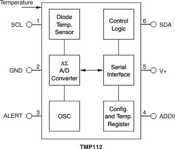
TMP112 TMP112D Block Diagram (SOT563 Package)Block Diagram (SOT563 Package)