SCEA149 September 2024 SN54SC245-SEP , SN54SC2T74-SEP , SN54SC3T97-SEP , SN54SC3T98-SEP , SN54SC4T00-SEP , SN54SC4T02-SEP , SN54SC4T08-SEP , SN54SC4T125-SEP , SN54SC4T32-SEP , SN54SC4T86-SEP , SN54SC6T06-SEP , SN54SC6T07-SEP , SN54SC6T14-SEP , SN54SC6T17-SEP , SN54SC8T138-SEP , SN54SC8T595-SEP , SN54SLC8T245-SEP
Abstract
Texas Instruments has historically only offered space-grade logic devices in larger ceramic packages, with many being released in the 1980s, 90s and early 2000s. Many of these older devices are also limited on supply voltage range, giving customers an option of either 3.3V or 5.0V Vcc. Rapidly emerging trends in the space industry for LEO (low-earth orbit) satellite platforms include the adoption of space-enhanced plastic (SEP) packaging over traditional ceramic packaging, as well as FPGAs (Field Programmable Gate Arrays) moving to lower supply voltages specifications such as 1.8V and even 1.2V. To best assist customers in designing next-generation space electronic systems, TI has released a brand-new group of SEP logic devices in the Space CMOS (SC) Logic family. This new family features readily available TID (total ionizing dose) + SEE (single event effects) radiation reports, 1.2V to 5.5V supply voltage support, and integrated single supply up/down level translation.
Introduction
As many modern LEO (Low-Earth Orbit) satellites are continuing to reduce in size, printed circuit board (PCB) size and power consumption limitations are rapidly becoming significant design roadblocks for many satellite system designers. Although some modern FPGAs have become smaller in size with lower voltage specifications and subsequent improvements in power efficiency, this has created additional issues. Smaller FPGAs can quickly become limited on GPIO (General Purpose Input/Output) and, more commonly, many surrounding peripheral devices remain restricted on I/O voltages, creating a so-called voltage mismatch. To solve these new design challenges, power-efficient and flexible interface designs are required.
A common type of interface design that has historically been sought after by satellite system designers is logic. Whether a buffer, level-translator, flip-flop, or shift register, these devices offer a reliable and cost-effective way to solve simple system design challenges and complete satellite designs. Dating back to the 1970s and 1980s, many engineers utilized Texas Instruments reliable 5V bipolar space logic devices to resolve various types of simple system design issues. While the majority of these logic devices are still available today, many of them have packages that are too large, or supply voltage specifications that are not compatible with many new FPGAs.
To both meet and exceed modern satellite system requirements, Texas Instruments performed a grounds-up development on a new Space CMOS (SC) Logic family, integrating a number of new features and benefits.
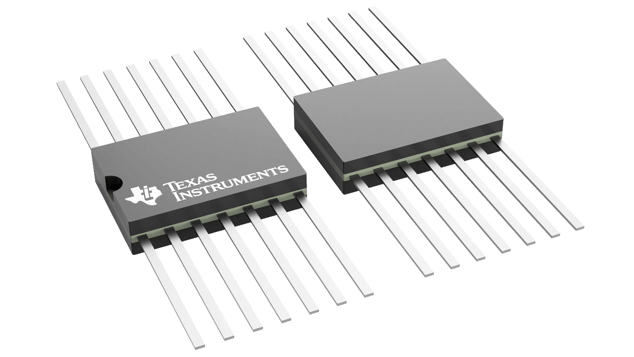 Figure 1 Bipolar Space Logic AND Gate
(SN54LS08-SP) in 14-pin CFP (W) Package
 New parameters and functions - TI Space CMOS Logic Family
- Wide supply voltage
specifications
The SC (Space CMOS) logic family was designed to interface with many different variations of system requirements and FPGA I/O voltages. Whether running at 5V, 3.3V or even 1.2V, the SC family is able to directly interface with FPGAs of various types and run off the same supply.
Table 1 Family Comparison Table by Supply Voltage Range (Recommended Operating Conditions)Common Logic Product Families Family AC ACT HC LS LVC SC (New!) Supply voltage - Min 2.0V 4.5V 2.0V 4.5V 1.65V 1.2V Supply voltage - Max 6.0V 5.5V 6.0V 5.5V 3.6V 5.5V - Integrated single supply up and down
level translation
When designing with FPGAs and lower supply voltages, one issue that many engineers encounter is known as a voltage mismatch between a system controller and peripheral device. For example, an FPGA can operate at a Vcc of 1.2V, while peripheral devices operate at 5V, 3.3V, or 1.8V logic levels. Especially if already using some sort of logic between these two devices, one can take advantage of the integrated level translation feature of the SCxT logic devices to solve this issue:
 Figure 2 Visual of Single Supply
Translation Feature of New Space Logic Products
 - Accessible
TID (Total Ionizing Dose) and SELU (Single Event Latch-Up) reports on ti.com
The SC family was designed with radiation tolerance in mind especially at lower supply voltages like 1.2 and 1.8V (30krad, 43MeV). Radiation data reports are readily available for the SC Family Logic devices on ti.com, as well as data sheet, inventory, and other design resources.
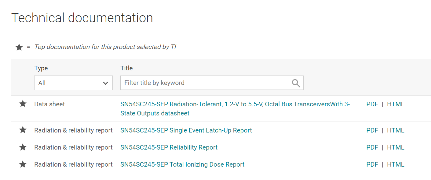 Figure 3 TI.com Technical Documentation
Section for Logic Space CMOS Family Devices
 - Smaller plastic packaging enables
significant board area savings and weight reduction
For lower-cost LEO missions, one constraint that many system designers have to work around is a smaller PCB size. Rather than trying to trim and form the leads of a larger ceramic package, TI logic offers the space CMOS family in a much smaller, plastic TSSOP packaging.
 Figure 4 Area Comparison Between Two
Ceramic Packages and the New Plastic Packages
 - New
pin-configurable logic functions enable increased system design flexibility
The SN54SC3T97-SEP and the SN54SC3T98-SEP are unique devices that allow for multiple logic functions within a singular chip. Especially when looking for logic early on in a design, these devices offer quick, cost-effective, and customizable designs to common system-level design issues.
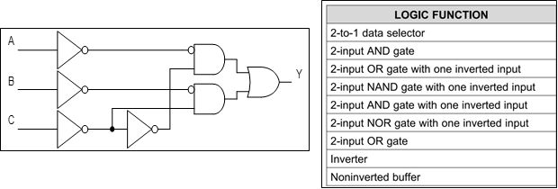 Figure 5 Logic Diagram and Function Table
for 97 Function (SN54SC3T97-SEP)
 - Integrated Triple Redundancy feature
for D-type Flip-Flop (SN54SC2T74-SEP) and other sequential devices
To best prevent SEUs (Single Event Upsets) and subsequent bit flipping, all sequential devices in the Space CMOS (SC) family such as flip-flops and shift registers come with an integrated triple modular redundancy feature. Where, each output of the sequential device is tied to a 3-channel majority voter-type circuit, and in the event of an upset of 1 channel, the 2 additional redundant paths allow the device to maintain functionality and signal integrity without failure.
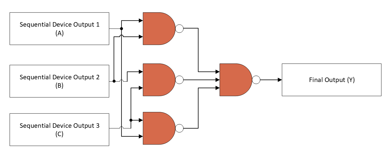 Figure 6 Triple Modular Redundancy Feature
Illustration (Majority State of A/B/C = Y)
Common applications of the SC family Logic in Satellite Payloads
- Logic AND gates (SN54SC4T08-SEP)
The SN54SC4T08-SEP is a 2-input, 4-channel AND gate with an integrated single-supply level translator. Many modern satellite payloads today utilize comparators to measure analog signals from various different types of sensors. Multiple logic gates are typically required to consolidate these comparator outputs and provide a single digital design to an MCU or FPGA. The added level translation feature allows for direct FPGA interface without the need for additional devices.
 Figure 7 SN54SC4T08-SEP Comparator
Consolidation Use Case
 - Octal BUS Transceiver (SN54SC245-SEP)
The SN54SC245-SEP is an Octal Bus Transceiver with 3-state outputs. With an output drive current up to 25mA, this device is excellent for driving digital signals across long board traces or transmission lines. The inputs can also accept voltages up to 5.5V, making the device capable of single supply down translation.
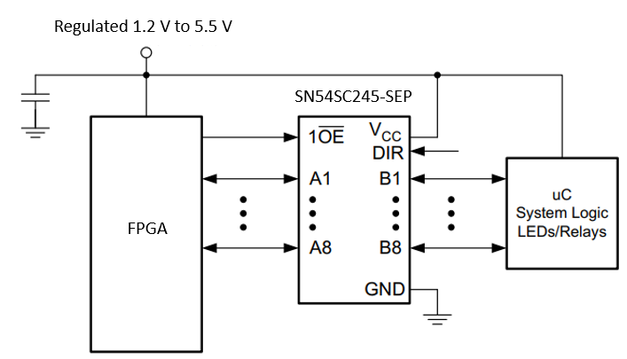 Figure 8 SN54SC245-SEP Driver Example Use
Case
 - Dual-Supply Voltage Level Translator
(SN54SLC8T245-SEP)
The SN54SLC8T245-SEP is a dual supply voltage level translator. This device resolves common voltage level mismatch between devices operating at the latest voltage nodes (0.7V, 0.8V, and 0.9V) and devices operating at industry standard voltage nodes (1.8V, 2.5V, and 3.3V). As modern FPGAs have moved to lower supply voltages, voltage translation type devices are becoming increasingly common in modern space systems.
 Figure 9 SN54SLC8T245-SEP Example Level
Translation Use Case
Product Selection Tables
| Logic and Voltage Translation - SEP Products | |||||
|---|---|---|---|---|---|
| Device | Function | Vcc | Channel # | TID and SEE ratings | TI.com link (Data sheet, Inventory, and Radiation Reports) |
| SN54SC4T00-SEP | NAND Gate | 1.2V to 5.5V | 4 |
50krad – Char. 30krad – RLAT 43MeV |
SN54SC4T00-SEP |
| SN54SC4T02-SEP | NOR Gate | 1.2V to 5.5V | 4 |
50krad – Char. 30krad – RLAT 43MeV |
SN54SC4T02-SEP |
| SN54SC6T06-SEP | Inverter; Open-Drain | 1.2V to 5.5V | 6 |
50krad – Char. 30krad – RLAT 43MeV |
SN54SC6T06-SEP |
| SN54SC6T07-SEP | Buffer; Open-Drain | 1.2V to 5.5V | 6 |
50krad – Char. 30krad – RLAT 43MeV |
SN54SC6T07-SEP |
| SN54SC4T08-SEP | AND Gate | 1.2V to 5.5V | 4 |
50krad – Char. 30krad – RLAT 43MeV |
SN54SC4T08-SEP |
| SN54SC6T14-SEP | Inverter; Schmitt-trigger | 1.2V to 5.5V | 6 |
50krad – Char. 30krad – RLAT 43MeV |
SN54SC6T14-SEP |
| SN54SC6T17-SEP | Buffer; Schmitt-trigger | 1.2V to 5.5V | 6 |
50krad – Char. 30krad – RLAT 43MeV |
SN54SC6T17-SEP |
| SN54SC4T32-SEP | OR Gate | 1.2V to 5.5V | 4 |
50krad – Char. 30krad – RLAT 43MeV |
SN54SC4T32-SEP |
| SN54SC2T74-SEP | D-type Flip-Flop | 1.2V to 5.5V | 2 |
50krad – Char. 30krad – RLAT 43MeV |
SN54SC2T74-SEP |
| SN54SC4T86-SEP | XOR Gate | 1.2V to 5.5V | 4 |
50krad – Char. 30krad – RLAT 43MeV |
SN54SC4T86-SEP |
| SN54SC3T97-SEP | Configurable multiple-function gate | 1.2V to 5.5V | 3 |
50krad – Char. 30krad – RLAT 43MeV |
SN54SC3T97-SEP |
| SN54SC3T98-SEP | Configurable multiple-function gate; inverted | 1.2V to 5.5V | 3 |
50krad – Char. 30krad – RLAT 43MeV |
SN54SC3T98-SEP |
| SN54SC4T125-SEP | Buffer; 3-state | 1.2V to 5.5V | 4 |
50krad – Char. 30krad – RLAT 43MeV |
SN54SC4T125-SEP |
| SN54SC8T138-SEP | 3-line to 8-line decoder/demultiplexer | 1.2V to 5.5V | 8 |
50krad – Char. 30krad – RLAT 43MeV |
SN54SC8T138-SEP |
| SN54SC245-SEP | Octal Bus Transceiver; 3-state | 1.2V to 5.5V | 8 |
50krad – Char. 30krad – RLAT 43MeV |
SN54SC245-SEP |
| SN54SLC8T245-SEP | Dual-Supply Voltage Translator | 0.65V to 3.6V | 8 |
20krad – Char. 20krad – RLAT 43MeV |
SN54SLC8T245-SEP |
| SN54SC8T541-SEP | Buffer; 3-state output | 1.2V to 5.5V | 8 |
50krad – Char. 30krad – RLAT 43MeV |
SN54SC8T541-SEP |
| SN54SC8T595-SEP | Shift Register | 1.2V to 5.5V | 8 |
50krad – Char. 30krad – RLAT 43MeV |
SN54SC8T595-SEP |