SLAAE75A November   2022  – March 2023 MSPM0L1105 , MSPM0L1106 , MSPM0L1303 , MSPM0L1304 , MSPM0L1304-Q1 , MSPM0L1305 , MSPM0L1305-Q1 , MSPM0L1306 , MSPM0L1306-Q1 , MSPM0L1343 , MSPM0L1344 , MSPM0L1345 , MSPM0L1346


  1.   Abstract
  2.   Trademarks
  3. MSPM0L Hardware Design Check List
  4. Power Supplies in MSPM0L Devices
    1. 2.1 Digital Power Supply
    2. 2.2 Analog Power Supply
    3. 2.3 Built-in Power Supply and Voltage Reference
    4. 2.4 Recommended Decoupling Circuit for Power Supply
  5. Reset and Power Supply Supervisor
    1. 3.1 Digital Power Supply
    2. 3.2 Power Supply Supervisor
  6. Clock System
    1. 4.1 Internal Oscillators
    2. 4.2 External Clock Output (CLK_OUT)
    3. 4.3 Frequency Clock Counter (FCC)
  7. Debugger
    1. 5.1 Debug Port Pins and Pinout
    2. 5.2 Debug Port Connection With Standard JTAG Connector
  8. Key Analog Peripherals
    1. 6.1 ADC Design Considerations
    2. 6.2 OPA Design Considerations
    3. 6.3 DAC Design Considerations
    4. 6.4 COMP Design Considerations
    5. 6.5 GPAMP Design Considerations
  9. Key Digital Peripherals
    1. 7.1 Timer Resources and Design Considerations
    2. 7.2 UART and LIN Resources and Design Considerations
    3. 7.3 I2C and SPI Design Considerations
  10. GPIOs
    1. 8.1 GPIO Output Switching Speed and Load Capacitance
    2. 8.2 GPIO Current Sink and Source
    3. 8.3 High Speed GPIOs
    4. 8.4 Open-Drain GPIOs Enable 5-V Communication Without a Level Shifter
    5. 8.5 Communicate With 1.8-V Devices Without a Level Shifter
    6. 8.6 Unused Pins Connection
  11. Layout Guides
    1. 9.1 Power Supply Layout
    2. 9.2 Considerations for Ground Layout
    3. 9.3 Traces, Vias, and Other PCB Components
    4. 9.4 How to Select Board Layers and Recommended Stack-up
  12. 10Bootloader
    1. 10.1 Bootloader Introduction
    2. 10.2 Bootloader Hardware Design Considerations
      1. 10.2.1 Physical Communication interfaces
      2. 10.2.2 Hardware Invocation
  13. 11References
  14. 12Revision History

Recommended Decoupling Circuit for Power Supply

It is recommended to connect a combination of a 10-μF plus a 100-nF low-ESR ceramic decoupling capacitor to the DVCC pin (see #FIG_MYT_TMC_GVB). Higher-value capacitors can be used but can impact supply rail ramp-up time. Decoupling capacitors must be placed as close as possible to the pins that they decouple (within a few millimeters).
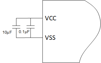
GUID-270BB8CA-3933-4FA4-9A9B-1174A4155891-low.png Figure 2-3 Power Supply Decoupling Circuit