SLAAEF9 November 2023 MSPM0C1104 , MSPM0G3507 , MSPM0L1227 , MSPM0L1227-Q1 , MSPM0L1228 , MSPM0L1228-Q1 , MSPM0L1306 , MSPM0L2227 , MSPM0L2227-Q1 , MSPM0L2228 , MSPM0L2228-Q1
- 1
- Abstract
- Trademarks
- 1MSPM0 Portfolio Overview
-
2Ecosystem And Migration
- 2.1 Ecosystem Comparison
- 2.2 Migration Process
- 2.3 Example
- 3Core Architecture Comparison
- 4Digital Peripheral Comparison
- 5Analog Peripheral Comparison
2.1.5 LaunchPad
Different from RL78 that has a Starter Kit, FPB and Target Board, LaunchPad development kits are the only evaluation modules for the MSPM0.
LaunchPad kits are easy-to-use EVMs that contain everything needed to start developing on the MSPM0. This includes an onboard debug probe for programming, debugging, and measuring power consumption with EnergyTrace™ technology. MSPM0 LaunchPad kits also feature onboard buttons, LEDs, and temperature sensors among other circuitry. Rapid prototyping is simplified by the 40-pin BoosterPack™ plug-in module headers, which support a wide range of available BoosterPack plug-in modules. You can quickly add features like wireless connectivity, graphical displays, environmental sensing, and more.
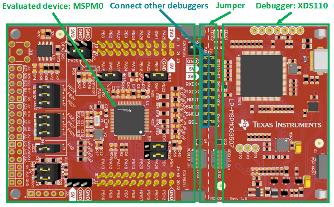
Figure 2-8 illustrates the LaunchPad overview. which contains the MCU and a XDS110 debugger. You can also use other debuggers like J-Link to debug the MCU after removing the jumpers.
 Figure 2-8 MSPM0G3507 Launchpad
Overview
Figure 2-8 MSPM0G3507 Launchpad
OverviewJumper isolation block contains Power(GND,5V,3.3V), UART(RXD, TXD), reset pin, arm debug channel(SWDIO,SWCLK) and BSL.
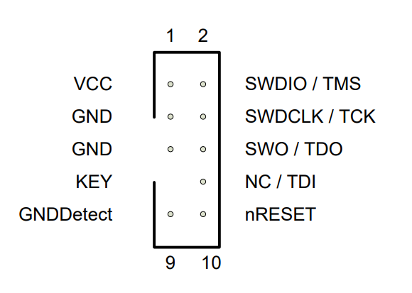
In addition to jumper caps, it is possible to burn using the standard Arm Cortex 10 pins connector (as shown in Figure 2-9 ) which is located on the right side of the Launchpad. The Cortex Debug Connector supports JTAG debug, Serial Wire debug and Serial Wire Viewer (via SWO connection when Serial Wire debug mode is used) operations.
 Figure 2-9 Arm Cortex 10-Pin
Definition
Figure 2-9 Arm Cortex 10-Pin
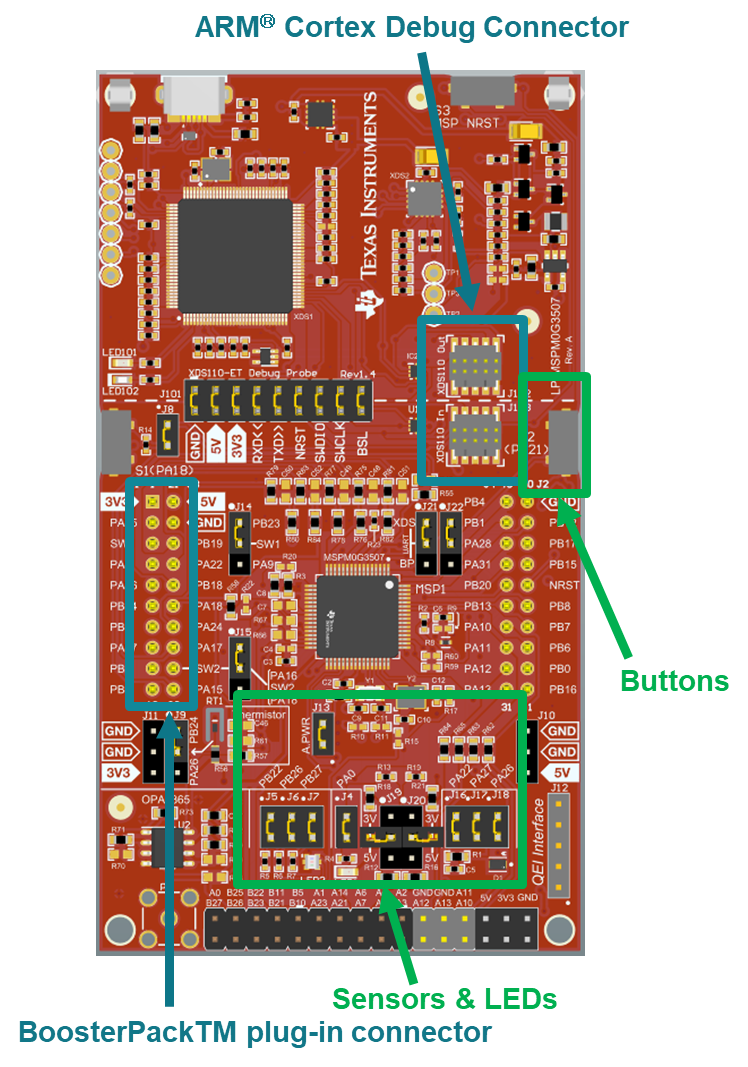
DefinitionFigure 2-10 shows some feature function of MSPM0G3507 Launchpad.
The lower sides of the Launchpad are the connectors of the booster pack, which are used to plug in specific functional modules directly and quickly build prototypes. In addition to this, it's also possible to use DuPont wire alone to lead out for quick use. The Launchpad has a user-defined button on each side, a temperature sensor, a light sensor, a monochrome LED, and an RGB LED underneath.
- LP-MSPM0G3507 LaunchPad development kit LP-MSPM0G3507 Evaluation board | TI.com
- LP-MSPM0L1306 LaunchPad development kit LP-MSPM0L1306 Evaluation board | TI.com
 Figure 2-10 MSPM0G3507 Launchpad Feature
Function