SLOA332A July 2023 – September 2024 LMV821-N , LMV831 , OPA2991 , OPA345 , OPA376 , OPA376-Q1 , OPA377 , OPA377-Q1 , OPA4991 , OPA991 , TL074 , TLV376 , TLV9001 , TLV9002 , TS321
- 1
- Abstract
- Trademarks
- 1 Slew Rate Definition
- 2 Bipolar Op Amp Slew Rate Example
- 3 CMOS Op Amp Slew Rate Example
- 4 Four Methods to Determine Boost or No Boost Using the Data Sheet
- 5 Slew Rate Dependencies on Circuit Signal Levels and Op Amp Gain Set by Feedback Network
- 6 How Much Output Slew Rate is Needed to Support a Sine Wave or Other Non-step Inputs
- 7 Stability Also Plays a Role in Observed Slew Rate
- 8 Summary
- 9 References
- 10Revision History
4.3 Method 3: Evaluate Large Signal Response
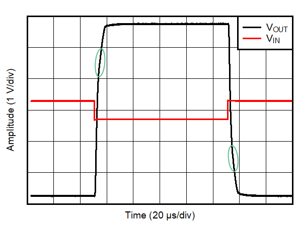
Use any large signal chart that has abrupt changes in rise and fall slopes, including charts called by another name, such as “Overload Recovery”. If a chart with these conditions can not be found, use the chart with the largest input signal. When looking at the transient response, select the slowest slew rate section that is more than 100mV of VID. Taking into account the noise gain (NG) of the circuit, the slowest slew rate section for a NG of 11 is 1.1V and for a NG of 1 the VID is 100mV. As shown in Figure 4-1 and Figure 4-2, the green ovals are the slowest slew rate with full VID. In both waveforms there is initially a faster slew rate. This initial increased slew rate can be caused by slew boost or internal parasitic capacitive feed-through. Typically, small rises come from capacitive feed-through and large rise come from slew boost. For the TLV9001 waveform, the selected area (SR) is 0.6V/µs, which is less than half of the data sheet slew rate of 2V/µs. Based on this information, slew boost is present in the TLV9001. For the LMV831 waveform, the selected area (SR) is 2.2V/µs rising and 1.8V/µs falling SR, which is close to the data sheet slew rate of 2V/µs; therefore, so no boost is expected.
| Boost | No Boost | |
|---|---|---|
| Device | TLV9001 | LMV831 |
| NG | 11 | 1 |
| VIN | 600mV | 500mV |
| Selected SR | 0.6V/μs | +2.2, -1.8V/μs |
| Data sheet SR | 2V/μs | 2V/μs |
 Figure 4-1 TLV9001 Overload
Recovery
 Figure 4-2 LMV831 Large Signal Step
Response With Gain = 1