SLOS930C November 2015 – October 2024 THS4541-Q1
PRODUCTION DATA
- 1
- 1 Features
- 2 Applications
- 3 Description
- 4 Device Comparison Table
- 5 Pin Configuration and Functions
-
6 Specifications
- 6.1 Absolute Maximum Ratings
- 6.2 ESD Ratings
- 6.3 Recommended Operating Conditions
- 6.4 Thermal Information
- 6.5 Electrical Characteristics: (Vs+) – Vs– = 5 V
- 6.6 Electrical Characteristics: (Vs+) – Vs– = 3 V
- 6.7 Typical Characteristics: 5-V Single Supply
- 6.8 Typical Characteristics: 3-V Single Supply
- 6.9 Typical Characteristics: 3-V to 5-V Supply Range
-
7 Parameter Measurement Information
- 7.1 Example Characterization Circuits
- 7.2 Frequency-Response Shape Factors
- 7.3 I/O Headroom Considerations
- 7.4 Output DC Error and Drift Calculations and the Effect of Resistor Imbalances
- 7.5 Noise Analysis
- 7.6 Factors Influencing Harmonic Distortion
- 7.7 Driving Capacitive Loads
- 7.8 Thermal Analysis
-
8 Detailed Description
- 8.1 Overview
- 8.2 Functional Block Diagram
- 8.3 Feature Description
- 8.4
Device Functional Modes
- 8.4.1
Operation from Single-Ended Sources to Differential Outputs
- 8.4.1.1 AC-Coupled Signal Path Considerations for Single-Ended Input to Differential Output Conversion
- 8.4.1.2 DC-Coupled Input Signal Path Considerations for Single-Ended to Differential Conversion
- 8.4.1.3 Resistor Design Equations for the Single-Ended to Differential Configuration of the FDA
- 8.4.1.4 Input Impedance for the Single-Ended to Differential FDA Configuration
- 8.4.2 Differential-Input to Differential-Output Operation
- 8.4.1
Operation from Single-Ended Sources to Differential Outputs
- 9 Application and Implementation
- 10Device and Documentation Support
- 11Revision History
- 12Mechanical, Packaging, and Orderable Information
7.1 Example Characterization Circuits
The THS4541-Q1 offers the advantages of a fully differential amplifier (FDA) design, with the trimmed input offset voltage of a precision op amp. The FDA is an extremely flexible device that provides a purely differential output signal centered on a settable output common-mode level. The primary options revolve around the choices of single-ended or differential inputs, ac-coupled or dc-coupled signal paths, gain targets, and resistor-value selections. The characterizations shown in Figure 6-1 to Figure 6-36 focus on single-ended-to-differential designs as the more challenging application requirement. Differential sources can certainly be supported and are often simpler to both implement and analyze.
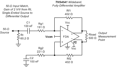
Because most lab equipment is single-ended, the characterization circuits typically operate with a single-ended, matched, 50-Ω input termination to a differential output at the FDA output pins. That output is then translated back to single-ended through a variety of baluns (or transformers) depending on the test and frequency range. DC-coupled, step-response testing uses two 50-Ω scope inputs with trace math. The starting point for any single-ended-to-differential, ac-coupled characterization plot is shown in Figure 7-1.
 Figure 7-1 AC-Coupled, Single-Ended Source to a Differential Gain of a 2-V/V Test Circuit
Most characterization plots fix the Rf (Rf1 = Rf2) value at 402 Ω, as shown in Figure 7-1. This element value is completely flexible in application, but the 402 Ω provides a good compromise for the parasitic issues linked to this value, specifically:
- Added output loading. The FDA appears like an inverting op amp design with both feedback resistors as an added load across the outputs (approximate total differential load in Figure 7-1 is 500 Ω || 804 Ω = 308 Ω).
- Noise contributions because of the resistor values. The resistors contribute both a 4kTR term and provide gain for the input current noise (see Section 7.5).
- Parasitic feedback pole at the input summing nodes. This pole created by the feedback R value and the 0.85‑pF differential input capacitance (as well as any board layout parasitic) introduces a zero in the noise gain, decreasing the phase margin in most situations. This effect must be managed for best frequency response flatness or step response overshoot. The 402-Ω value selected does degrade the phase margin slightly over a lower value, but does not decrease the loading significantly from the nominal 500-Ω value across the output pins.
The frequency domain characterization curves start with the selections of Figure 7-1. Then, various elements are modified to show the impact over a range of design targets, specifically:
- Gain setting is changed by adjusting Rt and the 2 – Rg elements (holding a 50-Ω input match).
- Output loading, including both resistive and capacitive load testing.
- Power-supply settings. Most often, a single +5-V test uses a ±2.5-V supply, and a +3-V test uses ±1.5-V supplies.
- The disable control pin is tied to Vs+ for any active channel test.
Because most network and spectrum analyzers are a single-ended input, the output network on the THS4541-Q1 characterization tests typically show the desired load connected through a balun to a single-ended, 50-Ω load, while presenting a 50-Ω source from the balun output back into the balun. For instance, Figure 7-2 shows a wideband MA/Com balun used for Figure 7-1. This network shows a 500-Ω differential load to the THS4541-Q1, but an ac-coupled, 50-Ω source to the network analyzer. Distortion testing typically uses a lower-frequency, dc-isolated balun (such as the TT1-6T) that is rotated 90° from the wider band interface of Figure 7-2.
 Figure 7-2 Example 500-Ω Load to a Single-Ended, Doubly-Terminated, AC-Coupled, 50-Ω Interface
This approach allows a higher differential load, but with a wideband 50-Ω output match at the cost of considerable signal-path insertion loss. This loss is acceptable for characterization, and is normalized out to show the characterization curves.
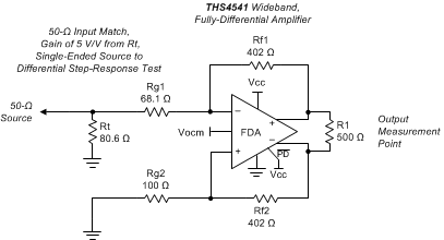
For time-domain or dc-coupled testing, the circuit
of Figure 7-3 is used as a starting point, where the gain of a
5-V/V
setting used in Figure 6-9 and Figure 6-27 are illustrated.
 Figure 7-3 DC-Coupled, Single-Ended-to-Differential, Basic Test Circuit Set for a Gain of 5 V/V
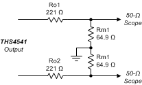
In this case, the input is dc-coupled, showing a 50-Ω input match to the source, gain of 5 V/V to a differential output, again driving a nominal 500-Ω load. Using a single supply, the Vocm control input can either be floated (defaulting to midsupply) or be driven within the allowed range for the Vocm loop (see the headroom limits on Vocm in the Electrical Characteristics tables). To use this circuit for step-response measurements, load each of the two outputs with a 250-Ω network, translating to a 50-Ω source impedance driving into two 50-Ω scope inputs. Then, difference the scope inputs to generate the step responses of Figure 6-9 and Figure 6-27. Figure 7-4 shows the output interface circuit. This grounded interface pulls a dc load current from the output Vocm voltage for single-supply operation. Running this test with balanced bipolar power supplies eliminates this dc load current and gives similar waveform results.
 Figure 7-4 Example 500-Ω Load to Differential, Doubly-Terminated, DC-Coupled 50-Ω Scope Interface