SLUAA04A june   2020  – may 2023 BQ25150 , BQ25155 , BQ25618 , BQ25619 , TS5A12301E , TS5A3157 , TS5A3159A , TS5A6542


  1.   1
  2.   High-Efficiency Charging for TWS Using a 2-Pin Interface
  3.   Trademarks
  4. Introduction
  5. System Overview
    1. 2.1 Charging Case
      1. 2.1.1 BQ25619
      2. 2.1.2 TLV62568P
      3. 2.1.3 TPS22910A
      4. 2.1.4 TS5A12301E
      5. 2.1.5 MCU
    2. 2.2 Earbuds
      1. 2.2.1 BQ25155
      2. 2.2.2 TPS22910A
      3. 2.2.3 TS5A12301E
      4. 2.2.4 BT/SOC
  6. Charging Case Algorithm Implementation
    1. 3.1 Initialization and Main Code
    2. 3.2 UART Interrupt and Output Voltage Adjustment
  7. Earbud Algorithm Implementation
    1. 4.1 Initialization and Main Code
    2. 4.2 Interrupt and Transmission
  8. Test Procedure
  9. Test Results
    1. 6.1 Dynamic Voltage Adjustment
    2. 6.2 BQ25619 with 4.6-V Output
    3. 6.3 Standard Boost with 5V Output
  10. Summary
  11. Schematics
  12. PCB Layout
  13. 10Software
    1. 10.1 Charging Case main.c
    2. 10.2 Earbuds main.c
  14. 11Revision History

Standard Boost with 5V Output

The third system is a baseline case that applies a standard 5 V on the case output. This system has sub-optimal performance for both efficiency and thermals.
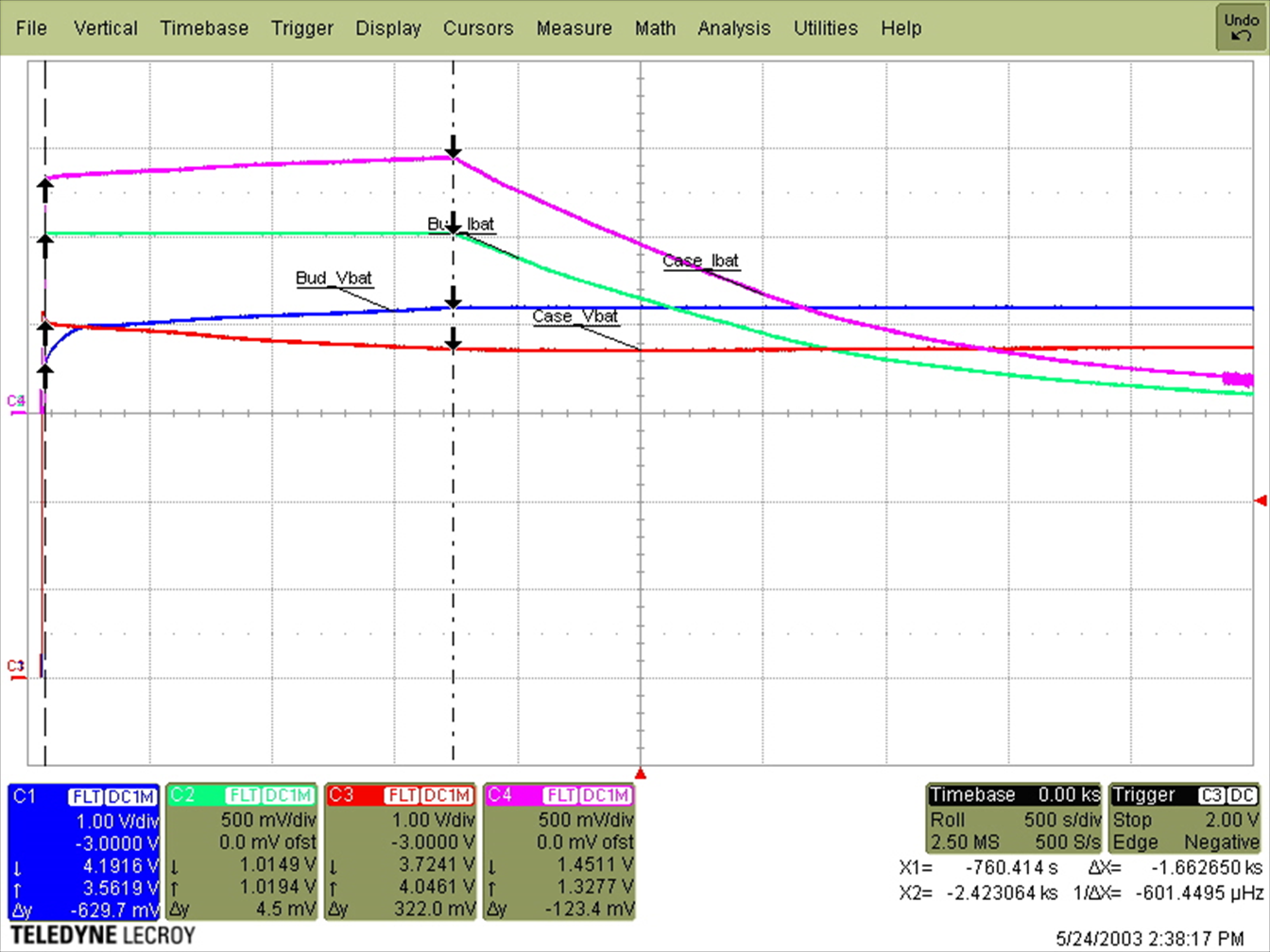
GUID-C36E2DFD-F92E-4CE3-94B2-2E1F58F4F132-low.pngFigure 6-5 Charge Cycle of the 5-V Output Design
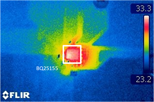
GUID-4C3C6FB6-7BB0-48A9-8D72-4BCC03E23B59-low.pngFigure 6-6 Thermal Performance of the 5-V Output Design