SLUAAH6 November 2021 UCC27424 , UCC27511 , UCC27517 , UCC27524 , UCC27531 , UCC27614 , UCC27624 , UCC27624-Q1
5 UCC27614 in a 400V to 12V DC-DC Converter
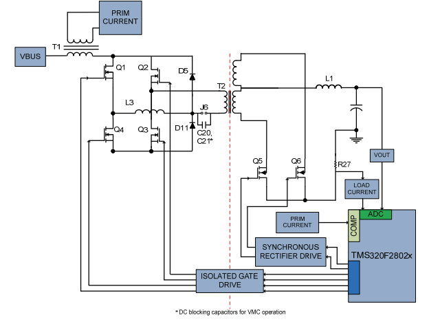
Figure 5-1 shows a simplified block diagram of the PSFB circuit where MOSFETs Q1, Q2, Q3 and Q4 form the phase shifted full-bridge on the primary side of the transformer T2. Q1 and Q4 are switched at 50 % duty and 180 degrees out of phase with each other. Similarly, Q2 and Q4 are switched at 50 % duty and 180 degrees out of phase with each other. The PWM signals for the half-bridge Q2 – Q3 are phase shifted with respect to those for second half-bridge Q1 – Q4. The amount of this phase shift dictates the amount of overlap between diagonal FETs, which in turn determines the amount of energy transferred.
 Figure 5-1 Simplified
Phase Shifted Full Bridge Converter with Secondary Side
Synchronous Rectification
Figure 5-1 Simplified
Phase Shifted Full Bridge Converter with Secondary Side
Synchronous RectificationSynchronous rectification is used for high output current isolated DC-DC to converters, where output diodes are replaced with MOSFETs to replace diode forward conduction losses with MOSFET conduction losses. This is because the voltage drop across a MOSFET, RDS(on), is significantly smaller than the diode forward voltage drop and therefore results in lower losses and higher efficiency.
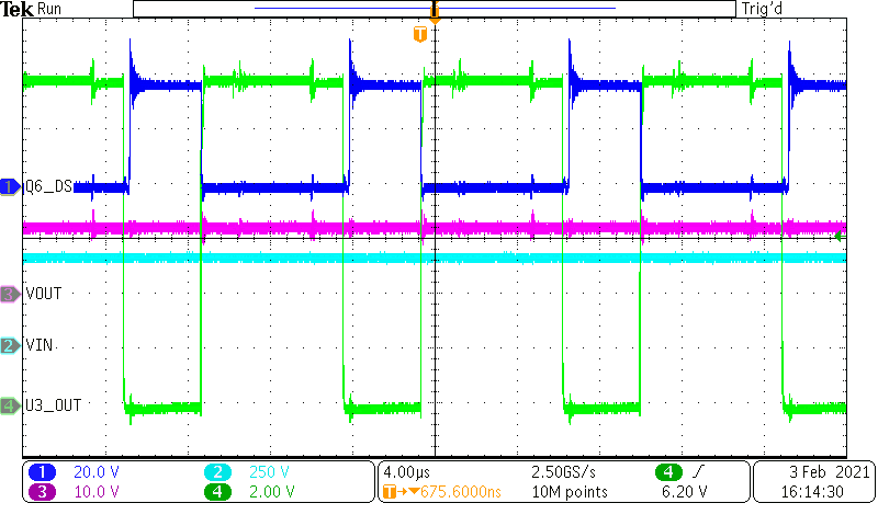
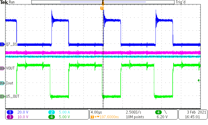
Figure 5-2 shows the converter input (400VDC), output (12VDC) using the UCC27614 outputs (CH4_U5_OUT) driving the synchronous rectification MOSFET to achieve efficient VDS switching times (CH1). Figure 5-3 shows the converter’s output voltage and current with a gate drive voltage of 12V to drive the synchronous rectification MOSFET.
 Figure 5-2 Converter Input, Converter Output, Gate Drive
Waveform, and MOSFET Drain to Source Voltage
 Figure 5-3 Converter Voltage Output, Converter Current Output,
Gate Drive Waveform, and MOSFET Drain to Source
Voltage