SLUU885C March   2012  – June 2024 UCD3138 , UCD3138064 , UCD3138064A , UCD3138128 , UCD3138A , UCD3138A64


  1.   1
  2.   2
  3.   Abstract
  4. Introduction
  5. Description
    1. 2.1 Typical Applications
    2. 2.2 Features
  6. Electrical Performance Specifications
  7. Schematics
  8. Test Setup
    1. 5.1 Test Equipment
    2. 5.2 Recommended Test Setup
  9. List of Test Points
  10. List of Terminals
  11. Test Procedure
    1. 8.1 Efficiency Measurement Procedure
    2. 8.2 Equipment Shutdown
  12. Performance Data and Typical Characteristic Curves
    1. 9.1 Efficiency
    2. 9.2 Power Factor
    3. 9.3 Total Harmonic Distortion (THD)
    4. 9.4 Input Current at 230 VAC and 50 Hz
    5. 9.5 Output Voltage Ripple
    6. 9.6 Output Turn On
    7. 9.7 Total Harmonic Distortion (THD)
    8. 9.8 Other Waveforms
  13. 10EVM Assembly Drawing and PCB Layout
  14. 11List of Materials
  15. 12Digital PFC Description
    1. 12.1  1PFC Block Diagram
      1. 12.1.1 Single-Phase PFC Block Diagram
      2. 12.1.2 2-Phase PFC Block Diagram
      3. 12.1.3 Bridgeless PFC Block Diagram
    2. 12.2  UCD3138 Pin Definition
      1. 12.2.1 UCD3138 Pin Definition in Single-Phase PFC
      2. 12.2.2 UCD3138 Pin Definition in 2-Phase PFC
      3. 12.2.3 UCD3138 Pin Definition in Bridgeless PFC
    3. 12.3  EVM Hardware – Introduction
      1. 12.3.1 PFC Pre-Regulator Input
      2. 12.3.2 PFC Power Stage
      3. 12.3.3 Non-Isolated UART Interface
      4. 12.3.4 Isolated UART Interface
      5. 12.3.5 Interface Connector of Control Card
      6. 12.3.6 UCD3138 Resource Allocation for PFC Control
    4. 12.4  EVM Firmware – Introduction
      1. 12.4.1 Background Loop
      2. 12.4.2 Voltage Loop Configuration
      3. 12.4.3 Current Loop Configuration
      4. 12.4.4 Interrupts
    5. 12.5  State Machine
    6. 12.6  PFC Control Firmware
    7. 12.7  System Protection
      1. 12.7.1 Cycle-by-Cycle Current Protection (CBC)
      2. 12.7.2 Over-Voltage Protection (OVP)
    8. 12.8  PFC System Control
      1. 12.8.1 Average Current Mode Control
      2. 12.8.2 ZVS and Valley Control
    9. 12.9  Current Feedback Control Compensation Using PID Control
      1. 12.9.1 Loop Compensation from Poles and Zeros in s-Domain
      2. 12.9.2 Feedback Loop Compenstaion Tuning with PID Coefficients
      3. 12.9.3 Feedback Loop Compensation with Multiple-Set of Parameters
    10. 12.10 Voltage Feedback Loop
  16. 13Evaluating the Single-Phase PFC with GUI
    1. 13.1 Graphical User Interface (GUI)
    2. 13.2 Open the Designer GUI
    3. 13.3 Overview of the Designer GUI
      1. 13.3.1 Monitor
      2. 13.3.2 Status
      3. 13.3.3 Design and Configure
  17. 14Monitoring, Re-configuring and Re-tuning with Designer GUI
    1. 14.1 Power On and Test Procedure
    2. 14.2 Monitoring with GUI
    3. 14.3 Configuration and Re-configuring with GUI
    4. 14.4 Feedback Control Loop Tuning and Re-Tuning with GUI
      1. 14.4.1 Current Loop Evaluation
      2. 14.4.2 Current Loop Re-Tuning
      3. 14.4.3 Voltage Loop Evaluation and Re-tuning
  18. 15Digital PFC Firmware Development
  19. 16References
  20. 17Revision History

Power On and Test Procedure

Power stage connection is the same as described earlier. Additionally to that setup, PMBus connection is required through USB-to-GPIO as shown in Figure 14-1.

After all connections are made, apply an AC source voltage with a specified value to the board AC input and refer to the other steps in the UCD3138PFCEVM-026 user’s guide. Open and start the “Fusion Digital Power Designer” GUI following the steps described in Section 13.2 and Section 13.3. Once PFC pre-regulator is up and running and the GUI is opened, then it is ready to use the Designer GUI to make evaluation.
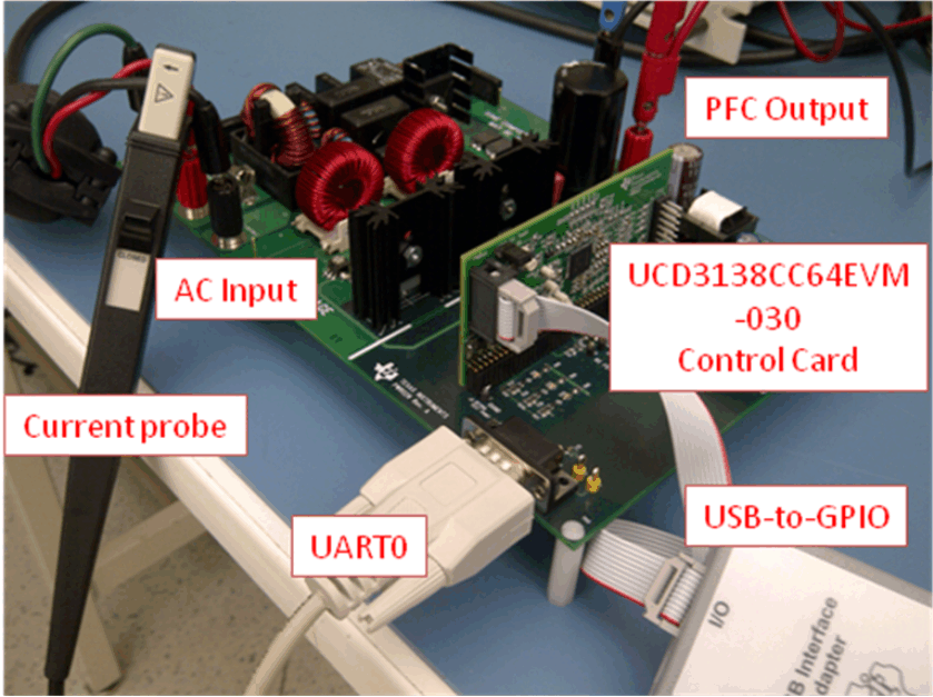
 Hardware Setup for Evaluation with Designer GUIFigure 14-1 Hardware Setup for Evaluation with Designer GUI