SLUU885C March   2012  – June 2024 UCD3138 , UCD3138064 , UCD3138064A , UCD3138128 , UCD3138A , UCD3138A64


  1.   1
  2.   2
  3.   Abstract
  4. Introduction
  5. Description
    1. 2.1 Typical Applications
    2. 2.2 Features
  6. Electrical Performance Specifications
  7. Schematics
  8. Test Setup
    1. 5.1 Test Equipment
    2. 5.2 Recommended Test Setup
  9. List of Test Points
  10. List of Terminals
  11. Test Procedure
    1. 8.1 Efficiency Measurement Procedure
    2. 8.2 Equipment Shutdown
  12. Performance Data and Typical Characteristic Curves
    1. 9.1 Efficiency
    2. 9.2 Power Factor
    3. 9.3 Total Harmonic Distortion (THD)
    4. 9.4 Input Current at 230 VAC and 50 Hz
    5. 9.5 Output Voltage Ripple
    6. 9.6 Output Turn On
    7. 9.7 Total Harmonic Distortion (THD)
    8. 9.8 Other Waveforms
  13. 10EVM Assembly Drawing and PCB Layout
  14. 11List of Materials
  15. 12Digital PFC Description
    1. 12.1  1PFC Block Diagram
      1. 12.1.1 Single-Phase PFC Block Diagram
      2. 12.1.2 2-Phase PFC Block Diagram
      3. 12.1.3 Bridgeless PFC Block Diagram
    2. 12.2  UCD3138 Pin Definition
      1. 12.2.1 UCD3138 Pin Definition in Single-Phase PFC
      2. 12.2.2 UCD3138 Pin Definition in 2-Phase PFC
      3. 12.2.3 UCD3138 Pin Definition in Bridgeless PFC
    3. 12.3  EVM Hardware – Introduction
      1. 12.3.1 PFC Pre-Regulator Input
      2. 12.3.2 PFC Power Stage
      3. 12.3.3 Non-Isolated UART Interface
      4. 12.3.4 Isolated UART Interface
      5. 12.3.5 Interface Connector of Control Card
      6. 12.3.6 UCD3138 Resource Allocation for PFC Control
    4. 12.4  EVM Firmware – Introduction
      1. 12.4.1 Background Loop
      2. 12.4.2 Voltage Loop Configuration
      3. 12.4.3 Current Loop Configuration
      4. 12.4.4 Interrupts
    5. 12.5  State Machine
    6. 12.6  PFC Control Firmware
    7. 12.7  System Protection
      1. 12.7.1 Cycle-by-Cycle Current Protection (CBC)
      2. 12.7.2 Over-Voltage Protection (OVP)
    8. 12.8  PFC System Control
      1. 12.8.1 Average Current Mode Control
      2. 12.8.2 ZVS and Valley Control
    9. 12.9  Current Feedback Control Compensation Using PID Control
      1. 12.9.1 Loop Compensation from Poles and Zeros in s-Domain
      2. 12.9.2 Feedback Loop Compenstaion Tuning with PID Coefficients
      3. 12.9.3 Feedback Loop Compensation with Multiple-Set of Parameters
    10. 12.10 Voltage Feedback Loop
  16. 13Evaluating the Single-Phase PFC with GUI
    1. 13.1 Graphical User Interface (GUI)
    2. 13.2 Open the Designer GUI
    3. 13.3 Overview of the Designer GUI
      1. 13.3.1 Monitor
      2. 13.3.2 Status
      3. 13.3.3 Design and Configure
  17. 14Monitoring, Re-configuring and Re-tuning with Designer GUI
    1. 14.1 Power On and Test Procedure
    2. 14.2 Monitoring with GUI
    3. 14.3 Configuration and Re-configuring with GUI
    4. 14.4 Feedback Control Loop Tuning and Re-Tuning with GUI
      1. 14.4.1 Current Loop Evaluation
      2. 14.4.2 Current Loop Re-Tuning
      3. 14.4.3 Voltage Loop Evaluation and Re-tuning
  18. 15Digital PFC Firmware Development
  19. 16References
  20. 17Revision History

Bridgeless PFC Block Diagram

A function block diagram of a bridgeless PFC is shown in Figure 27. The digital controlled bridgeless PFC has a same power stage as those seen in analog controlled. All signals interacted with UCD3138 are explained in the section Section 12.2.
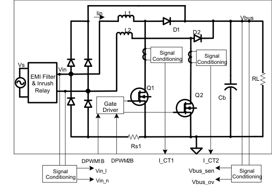
 Digitally Controlled Bridgeless PFC System Block DiagramFigure 12-3 Digitally Controlled Bridgeless PFC System Block Diagram