SLVAFJ3 september 2023 LM5177 , LM51772
2.2 Optimizing Hot Loops in the Power Stage
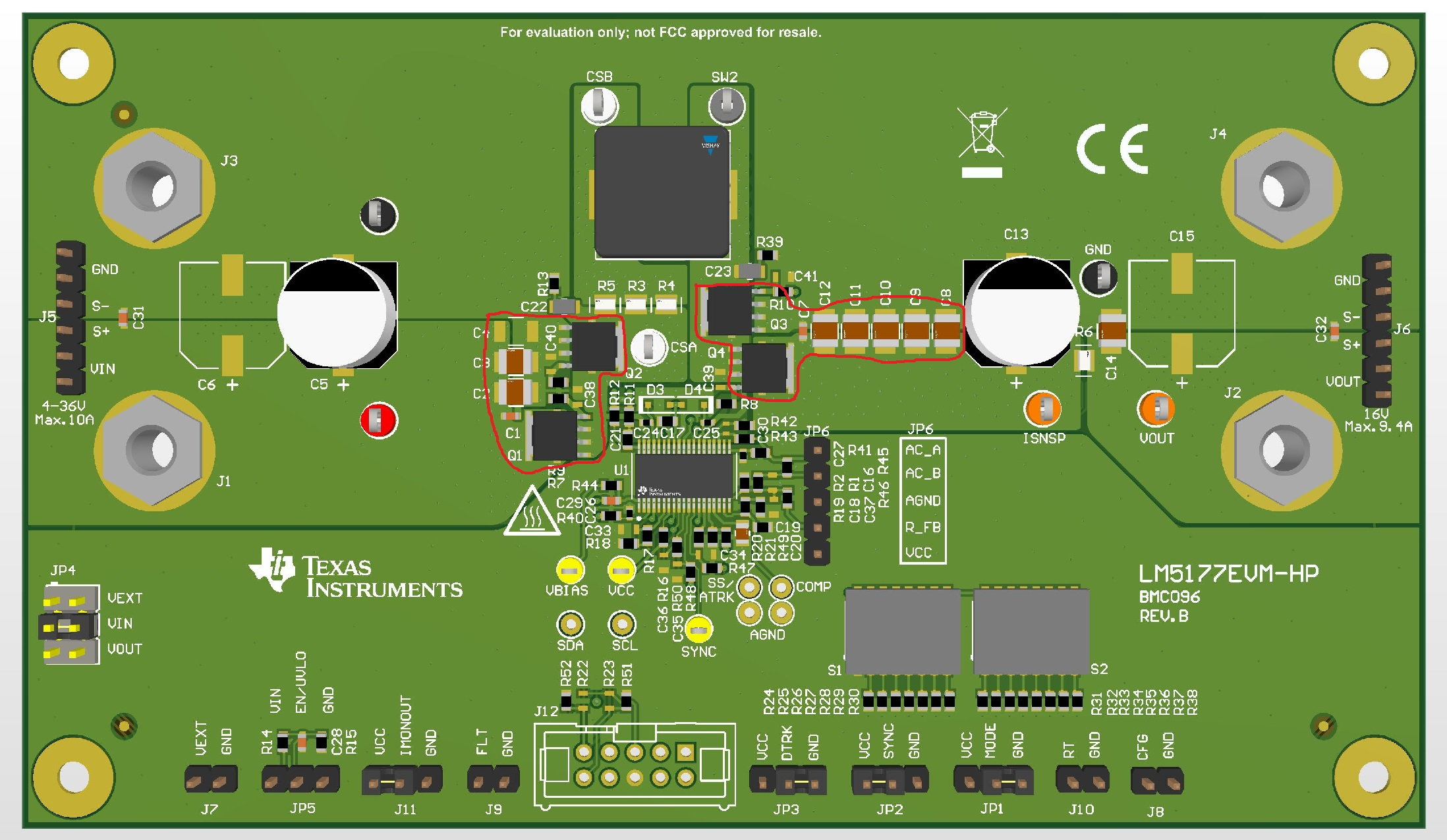
Once you have identified the critical parts of your power supply layout, your next task is to minimize any sources of noise and unwanted parasitic. The input-switching current loop and output-switching current loop are the dominant high current loops. Minimize the area of these loops to suppress generated switching noise and optimize switching performance.
The most important loop areas to minimize are the path from the input capacitors through the buck high-side and low-side MOSFETs, and back to the ground connection of the input capacitor and the path from the output capacitors through the boost high-side and low-side MOSFETs, and back to the ground connection of the output capacitor. Connect the negative terminal of the capacitor close to the source of the low-side MOSFETs (at ground). Similarly, connect the positive terminal of the capacitor or capacitors close to the drain of the high-side MOSFETs of both loops.
In addition to these recommendations, follow any layout considerations of the MOSFETs as recommended by the MOSFET manufacturer, including pad geometry and solder paste stencil design.
 Figure 2-2 Hot Loops in a LM5177 Four
Switch Buck - Boost Device