SLVAFP1 February 2024 TPS54KB20
2 Butterfly Footprint Analysis
The butterfly-style footprint is a unique feature to the
TPS54KB2x that distinguishes the device from predecessor and competitor devices. The TPS54KB2x
features two VIN ports parallel from across the IC package, and two PGND planes similarly
parallel so that it resembles the shape of a butterfly, hence the name. The layout method
carries advantages as it minimizes parasitics and noise. The parallel VIN and GND planes play
a significant role in reducing the excess amounts of unwanted resistance and inductance. In
addition, this high power density footprint allows for further performance enhancements
including slightly increased efficiency, reduced switch-node ringing, and thermal/electrical
specification refinement. In terms of layout area, the TPS54KB2x offers reduction in design
size compared to its predecessor part due to the butterfly footprint's ability to compress
component placement on the layout.
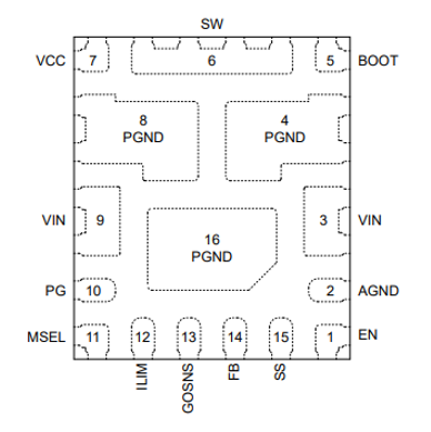
 Figure 2-1 Butterfly-Style Outline
 Figure 2-1 Butterfly-Style Outline
Figure 2-1 presents how the distinctive symmetrical layout appears in a pinout format. As previously mentioned, the footprint consists of two parallel VIN rails and two parallel PGND planes divided by the package symmetrically which aids in the reduction of parasitics. Furthermore, the butterfly footprint arranges the input capacitors in such a way that magnetic field cancellation occurs, leading to loop inductance being decreased.
Section 2.1 and Section 2.2 briefly show the efficiency and thermal advantages of TPS54KB20 compared to its predecessor part, TPS54JB20.