SLVU944B October   2015  – October 2020 TPS7H1101-SP


  1.   Trademarks
  2. 1Introduction
    1. 1.1 Related Documentation
  3. 2Description
  4. 3Test Setup
    1. 3.1 Equipment
      1. 3.1.1 Power Supplies
      2. 3.1.2 Load Number 1
      3. 3.1.3 Meters
      4. 3.1.4 Oscilloscope
    2. 3.2 Bench Test Setup Conditions
      1. 3.2.1 Headers Description and Jumper Placement
      2. 3.2.2 Testing
    3. 3.3 Power-Up Procedure
      1. 3.3.1  IOUT and VOUT Measurements
      2. 3.3.2  Output Current Limiting
      3. 3.3.3  High-Side Current Sense
      4. 3.3.4  Current Foldback
      5. 3.3.5  Power Good
      6. 3.3.6  Dropout Voltage
      7. 3.3.7  Transient Response
      8. 3.3.8  Current Sharing
      9. 3.3.9  Soft-Start
      10. 3.3.10 Enable and Disable
      11. 3.3.11 Turn-Off
  5. 4Board Layout
    1. 4.1 EVM Layout Flexibility
  6. 5Schematic and Bill of Materials
  7.   Revision History

High-Side Current Sense

Monitoring the voltage at the CS pin will indicate voltage proportional to the output current. Figure 3-4 shows typical curve VCS vs IOUT for Vin = 2.28 V and R23 = 3.65 kΩ. A resistor connected from current sense (CS) pin to VIN indicates voltage proportional to the output current.
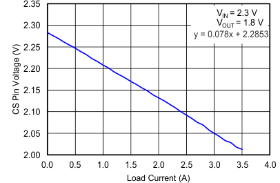
GUID-33E32B2A-530B-4683-B5E8-568B2F0BA5B1-low.gifFigure 3-4 VCS (V) vs IOUT (A)

Monitoring current in CS pin (ICS vs IOUT) indicates the current sense ratio between the main PMOSFET and the current sense MOSFET as shown in Figure 3-5. This plot shows that the CSR ratio is independent of VCS voltage. Note that VCS must be above 0.3V to insure proper biasing, and also must be greater than 0.9 x VREF (0.544 V) to have foldback current limit enabled.
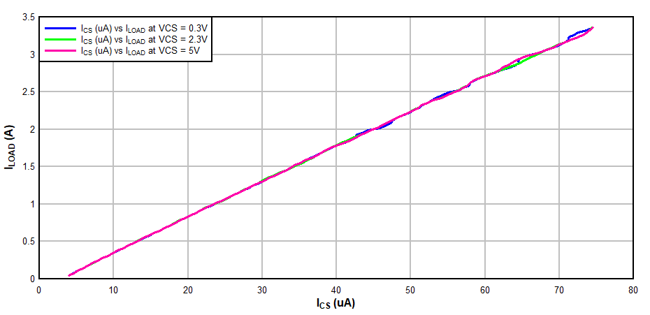
GUID-D7C6A4D4-8220-45F8-B021-647618148A30-low.gif Figure 3-5 IOUT (A) vs ICS (A)