SLYY193C january 2023 – april 2023 LMQ61460-Q1 , TPS54319 , TPS62088 , TPS82671 , UCC12040 , UCC12050
- At a glance
- Authors
- 3
- What is power density?
- What limits power density?
- What limits power density: switching losses
- Key limiting factor No. 1: charge-related losses
- Key limiting factor No. 2: reverse-recovery losses
- Key limiting factor No. 3: turn-on and turn-off losses
- What limits power density: thermal performance
- How to break through power density barriers
- Switching loss innovations
- Package thermal innovations
- Advanced circuit design innovations
- Integration innovations
- Conclusion
- Additional resources
Integration innovations
The final piece of the puzzle toward the best power density is integration. Cost-effective integration reduces parasitics, reduces the bill of materials, enables higher efficiency and saves space. Integration applies to several aspects of power management. It can entail including more electrical circuits in an IC, adding more components in a package, or packing more in the power solution through other physical or mechanical means. A few examples of technology leadership in this area are drivers integrated with GaN FETs, capacitor integration for critical loop inductance reduction, and 3D stacking of passive components.
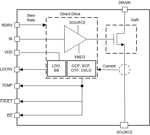
Including gate drivers with switching power FETs has many benefits. The switching gate-drive loop inductance decreases, which enables higher switching speeds, more robust operation and fewer components. GaN FETs in particular benefit from this integration. Additional features like overcurrent protection, overtemperature protection and monitoring are included in devices like the LMG3522R030-Q1 (see Figure 22). This integration significantly simplifies the power-management solution and enables designers to achieve all that GaN has to offer.
 Figure 22 Driver, protection and
monitoring functions integrated with a GaN switch on the LMG3522R030-Q1.
Figure 22 Driver, protection and
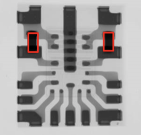
monitoring functions integrated with a GaN switch on the LMG3522R030-Q1.Another avenue of integration is including passive components in the IC package. Integrating high-frequency decoupling capacitors is one technique used in the LMQ61460-Q1, shown in Figure 23. Integrating the capacitors can improve efficiency by reducing critical loop parasitic inductance and reduce EMI. This power solution can also increase switching times without sacrificing system robustness or exceeding thermal limits, leading to higher switching frequencies and solution size reductions with less EMI filtering. The UCC14240 leverages magnetic component integration to provide an isolated bias supply without an external transformer. This approach reduces size, complexity and EMI.
 Figure 23 X-ray photograph of the
LMQ61460-Q1, with the integrated bypass capacitors highlighted.
Figure 23 X-ray photograph of the
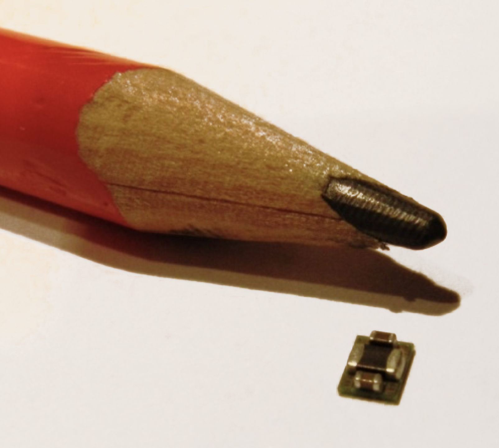
LMQ61460-Q1, with the integrated bypass capacitors highlighted.A final example of integration is 3D stacking of components, which occurs often in power modules with integrated passive components. Figure 24 uses the TPS82671 as an example. This device embeds the power IC in a laminate substrate and places an inductor and input and output capacitors on top. This incredibly small solution does not require additional components. A simple integration concept can achieve amazing results, saving PCB area and simplifying the power solution.
 Figure 24 Tiny power module with an
integrated power IC, inductor and capacitors.