-
Time-Saving and Cost-Effective Innovations for EMI Reduction in Power Supplies SLYY200A April 2021 – December 2023 LM25149 , LM25149-Q1 , LM5156-Q1 , LM5157-Q1 , LM53635-Q1 , LM60440-Q1 , LM61460-Q1 , LM61495-Q1 , LMQ62440-Q1 , LMR33630-Q1 , LMS3655-Q1 , TPS55165-Q1 , UCC12040 , UCC12050
-
Time-Saving and Cost-Effective Innovations for EMI Reduction in Power Supplies
- 1
- Overview
- At a glance
- What is EMI?
- Conventional methods to reduce EMI in the low- and high-frequency ranges
- Innovations in reducing low-frequency emissions
- Spread spectrum
- Active EMI filtering
- Cancellation windings
- Innovations in reducing high-frequency emissions
- HotRod™ package
- Enhanced HotRod QFN
- Integrated input bypass capacitor
- True slew-rate control
- EMI modeling capabilities
- Low-frequency EMI designs using WEBENCH® design tool
- Conducted and radiated EMI results published in data sheets
- Conclusion
- Keep product categories for low EMI
- IMPORTANT NOTICE
Time-Saving and Cost-Effective Innovations for EMI Reduction in Power Supplies
At a glance
| 1 What is EMI? | EMI is electromagnetic energy — produced as an undesirable byproduct of
switching currents and voltages — that comes from a variety of physical
phenomena and manifests during stringent EMI tests. |
| 2 Conventional methods to reduce EMI in the low- and high-frequency ranges | Reducing EMI is an endeavor plagued with trade-offs. Conventional methods to
reduce EMI include using large, expensive filters or reducing switching slew
rates, a technique that directly impacts efficiency. |
| 3 Innovations in reducing low-frequency emissions | To realize all of the benefits of a switchmode power supply, it is paramount
for EMI reduction techniques to resolve the traditional trade-offs. This
requires creative solutions for both low- and high-frequency EMI, as well as
accurate modeling techniques. |
What is EMI?
In a system that requires electromagnetic compatibility (EMC), components acting as electromagnetic sources are designed to reduce their interference, and components that are susceptible to interference are designed to reduce their susceptibility. When end-equipment manufacturers integrate components from various suppliers, the only way to ensure that the interferers and susceptible circuits can peacefully coexist is through the establishment of a common set of rules, where interference is limited to a certain level, and susceptible circuits are capable of handling that level of interference.
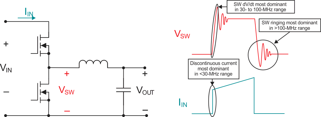 Figure 1 Example of EMI sources in an
SMPS.
Figure 1 Example of EMI sources in an
SMPS.These rules are established in industry-standard specifications such as Comité International Spécial des Perturbations Radioélectriques (CISPR) 25
for the automotive industry, and CISPR 32 for multimedia equipment. CISPR standards are critical for EMI design, as they will dictate the targeted performance of any EMI mitigation technique. This paper’s focus will be on reducing interference, as the SMPS is typically the electromagnetic interferer. For a comprehensive list of EMI standards, see An overview of conducted EMI specifications for power supplies and An overview of radiated EMI specifications for power supplies.
In addition to knowing the appropriate standard for a given application, it is also important to understand how to measure EMI, as this knowledge will give you insight into reducing EMI. EMI measurements are typically divided into conducted and radiated, which reveal both the method of measurement and how the EMI was generated. Although conducted emissions are typically associated with lower frequencies (<30 MHz) and radiated emissions are typically associated with higher frequencies (>30 MHz), the distinction between the two is not quite so simple, as conducted and radiated frequency ranges do overlap.
Conducted emissions measurements are designed to quantify the EMI generated from a device and returned to its power source. It’s important to reduce these emissions for many applications, as it is common for other sensitive circuits to connect to the same power-supply lines. Reducing conducted EMI is particularly important when dealing with long wire harnesses, which are increasing in number in modern automobiles.
Figure 2 shows a generic test setup for conducted emissions, including a power source, line impedance stabilization network (LISN), EMI receiver, supply wires and a device under test (DUT). The LISN plays a key role, acting as a low-pass filter that ensures the repeatability and comparability of EMI measurements, and providing a precise impedance to the DUT. Figure 2 also illustrates an important subdivision of conducted emissions into common-mode (CM) and differential- mode (DM) currents. DM currents flow between the power-supply line and its return path, and are the dominant factor at lower frequencies. CM currents flow between each of the power lines and ground, and are the dominant factor at higher frequencies.
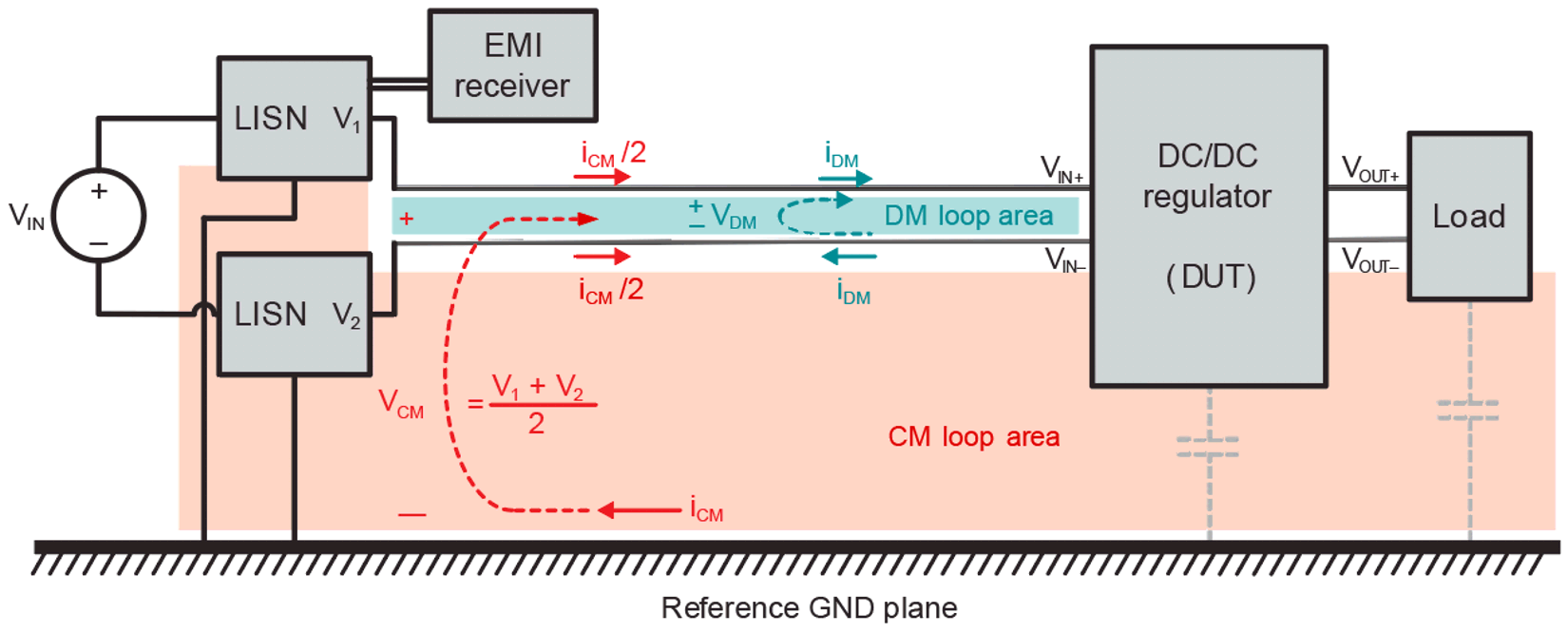 Figure 2 Generic test setup for conducted emissions measurements, with DM and CM loops
highlighted in teal and red, respectively.
Figure 2 Generic test setup for conducted emissions measurements, with DM and CM loops
highlighted in teal and red, respectively.Radiated measurements have a setup similar to conducted measurements; the main difference is that the EMI receiver is not connected directly to the LISN but to a nearby antenna. Radiated energy in an SMPS comes from fast transient current loops generating magnetic fields, and fast transient voltage surfaces generating electric fields. Because the same current loops that generate radiated magnetic fields also generate DM conducted emissions, and the same surfaces that generate radiated electric fields also generate CM conducted emissions, many EMI mitigation techniques reduce both conducted and radiated emissions, but may be targeted specifically for one or the other.
In general, lower-frequency emissions are mitigated by using large passive filters, which add board area and cost to the solution. High-frequency emissions present different challenges in terms of measurement, modeling and mitigation, primarily as a result of their parasitic nature. Common mitigation techniques for high-frequency emissions include controlling slew rates and reducing parasitics. Figure 3 summarizes the mitigation techniques contained in this paper, the frequency bands in which they are most beneficial and an example of the frequency ranges covered by the CISPR 25 standard.
Conventional methods to reduce EMI in the low- and high-frequency ranges
Input voltage ripple generated by discontinuous currents in an SMPS can conduct to other systems when the systems share common physical contacts. Without proper mitigation, excessive input or output voltage ripple can compromise operation of the source, load or adjacent system. Traditionally, you could minimize the input ripple by using a passive inductor-capacitor (LC)-based EMI filter, as shown in Figure 4. An LC filter offers the required attenuation necessary to meet EMI specifications. The trade-off is a size and cost penalty for the system depending on the required attenuation, which will lower the overall power density. Also, large-sized inductors for input EMI filter design lose attenuation at frequencies greater than 30 MHz because of their lower self-resonant frequency, necessitating additional components like ferrite beads to handle the high-frequency attenuation.
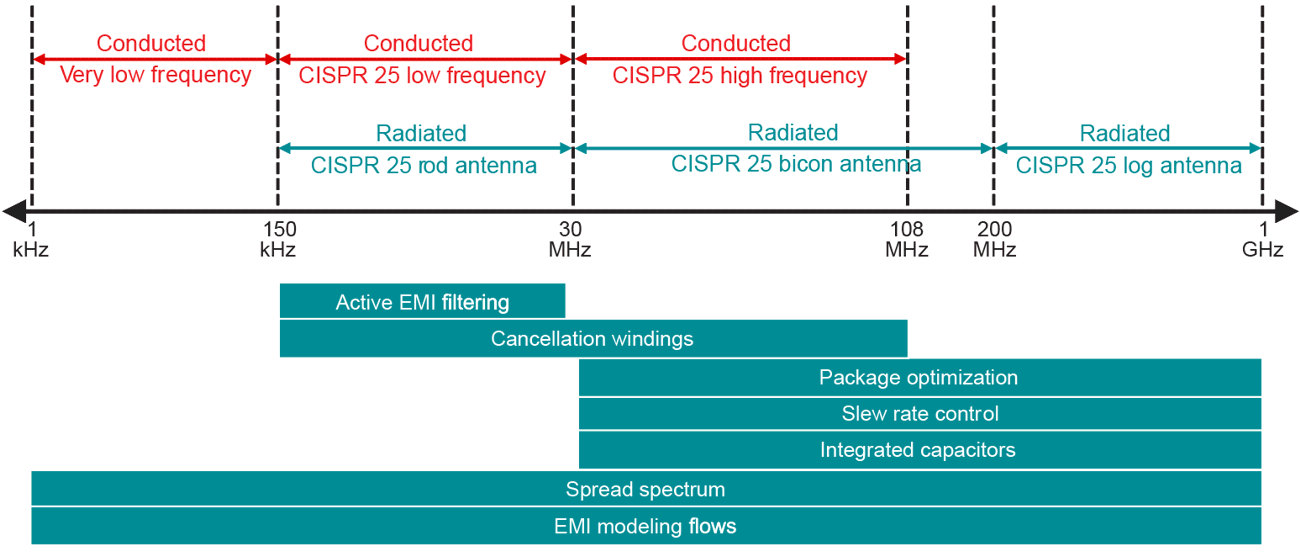 Figure 3 A summary of the EMI mitigation techniques presented in this paper.
 Figure 4 A typical LC-based passive filter for EMI reduction, along with the
attenuation obtained.
Figure 4 A typical LC-based passive filter for EMI reduction, along with the
attenuation obtained.Another conventional approach to mitigating EMI is to use spread spectrum (or clock dithering) to modulate the switching frequency of an SMPS, which will reduce peaks in the frequency spectrum associated with the fundamental switching frequency and its harmonics — but at the expense of an increased noise floor, as shown in Figure 5.
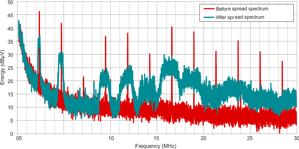 Figure 5 Example of the frequency spectrum of an SMPS with and without spread
spectrum.
Figure 5 Example of the frequency spectrum of an SMPS with and without spread
spectrum.Spread spectrum is an attractive technique, given its ease of implementation and the fact that you can use it in conjunction with other EMI reduction methods. It is not a panacea, however, as it can only provide relative reductions to existing EMI, and by nature its performance diminishes with lower switching frequencies. Furthermore, you can traditionally only apply spread spectrum to a single frequency band, for reasons that we will explore in the next section.
To minimize the size of the filter inductors, you can choose higher switching frequencies for your SMPS design. It is important to avoid sensitive frequency bands for switcher operation, however. For example, the preferred switching frequency for automotive power solutions has traditionally been in the sub-AM bands (approximately 400 kHz). Choosing a higher switching frequency to minimize inductor size means that you must avoid the entire AM band (525 to 1,705 kHz) so as to not have fundamental switching spurs in the more stringent automotive EMI frequency bands.
Switching converters from Texas Instruments (TI) have a switching frequency above 1.8 MHz to satisfy the EMI band requirements. The push to higher switching frequencies imposes a severe restriction on the switching transition rise and fall times to reduce switching losses. However, a switch node with very short rise and fall times maintains high energy content even at high frequencies close to its 100th harmonic, as shown in Figure 6, again highlighting the trade-off between high efficiency and low EMI.
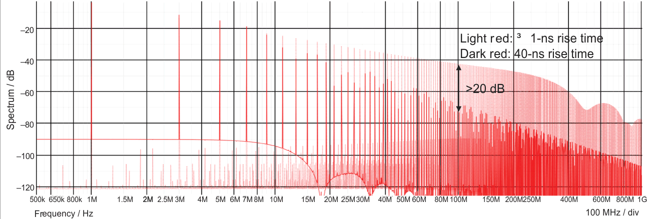 Figure 6 EMI plots of square waveforms with different rise times.
High slew rates will additionally result in high-frequency switch-node ringing, due to the presence of parasitic inductances in the power path of DC/DC converters, which further increases emissions at the ringing frequency and above. Figure 8 shows how the slew rate and the associated ringing on the switch node affect emissions. The traditional way to limit EMI emissions caused by the switching transition is to slow them down by adding intentional resistance in the gate-drive path of the switching device. This causes the transitions to happen more slowly, leading to faster roll-off of the emissions and an 8- to 10-dB reduction in emissions at the ringing frequency. This slowdown of the switching edges comes with a penalty of 2% to 3% in the peak current efficiency of the switching converter, however.