SNLA433A August 2023 – December 2024 DS320PR1601 , DS320PR410 , DS320PR810 , SN75LVPE5412 , SN75LVPE5421
4 PCIe Warm Resets
In applications where the redriver is operated in an I2C mode and can be configured by an external controller, it is common to perform redriver tuning in a live environment where the redriver and other system elements maintain power and new EQ settings can be written directly to the device. This is convenient, not needing a power cycle compared to when changes are applied to EEPROM or a board hardware reconfiguration if the device is operated in pin mode.
However, if the redriver testing procedure involves a live PCIe link, then it is important to perform a warm reset of the link before evaluating the signal quality through lane margining and similar tests. Both the PCIe transmitter sending signals to the redriver, and the PCIe receiver that the redriver outputs signals to, have their own settings relating to signal conditioning that are automatically negotiated and calibrated during the link training process. For example, the transmitter is expected to automatically evaluate various PCIe presets applied to transmitted data and select one for use. When the redriver settings are changed while the link is in a normal operational state (L0), the electromagnetic characteristics of the channel are now different, but the transmitter does not dynamically re-evaluate and renegotiate its chosen PCIe preset in response. It is possible that the PCIe preset setting held from the initial negotiations can be sub-optimal for the new channel conditions. To address this, performing a warm reset causes the link to be renegotiated, and since the system power is maintained, the redriver keeps its adjusted EQ settings. Depending on the type of system being tested, a warm reset can be performed by running a relevant PCIe protocol command in CPU configuration software, or alternatively by performing a warm reboot of the operating system or BIOS.
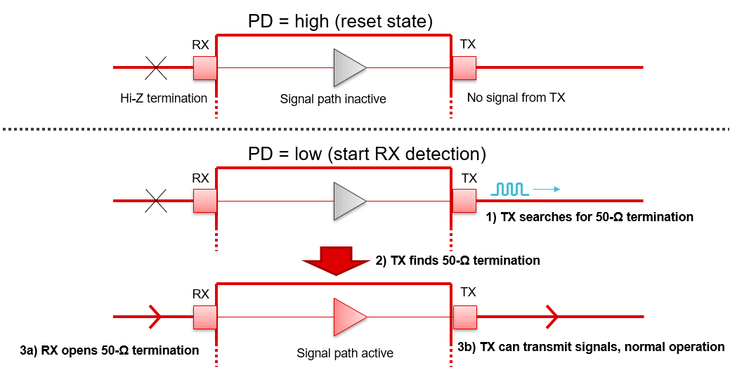
Although warm resets are performed at a protocol level and a protocol-agnostic redriver has relatively little involvement, it is helpful to make sure that the board design that the RX detection subsystem of the redriver is cleared and reactivated in sync with the other PCIe devices during a warm reset and similar conditions by manipulating the PD pin. The operation of the redriver RX detection in relation to the PD pin is shown in Figure 4-1.
 Figure 4-1 Redriver RX Detection Functionality
The redriver is positioned in the middle of the link and is expected to act like a middleman for RX detection sequencing, showing 50Ω terminations on the redriver RX pins only when the redriver TX pins on the other side have successfully detected 50Ω terminations from the device they are facing. That device whose RX is connected to the redriver TX is expected to only enable the 50Ω terminations when the internal startup is fully complete and it is ready to begin PCIe negotiations. If the redriver does not clear the RX terminations after a warm reset and wait until the appropriate conditions to turn them on, the root complex may see the redriver's terminations immediately (the moment it starts to look) and then begin PCIe negotiations when the endpoint may not be completely ready. This can increase the risk of linkup problems.
Synchronizing the redriver RX detection process to the control of the PCIe protocol is done by connecting the PD pin to an inverted version of the PCIe PERST# signal. PERST# is held low when the link is in reset (either a warm reset or power-on reset) and during this time the inverted connection to PD holds the redriver in reset with RX terminations cleared. The transition from low to high indicates to all PCIe devices that the linkup process needs to be initiated, and the redriver's role is to start searching for terminations at TX pins.
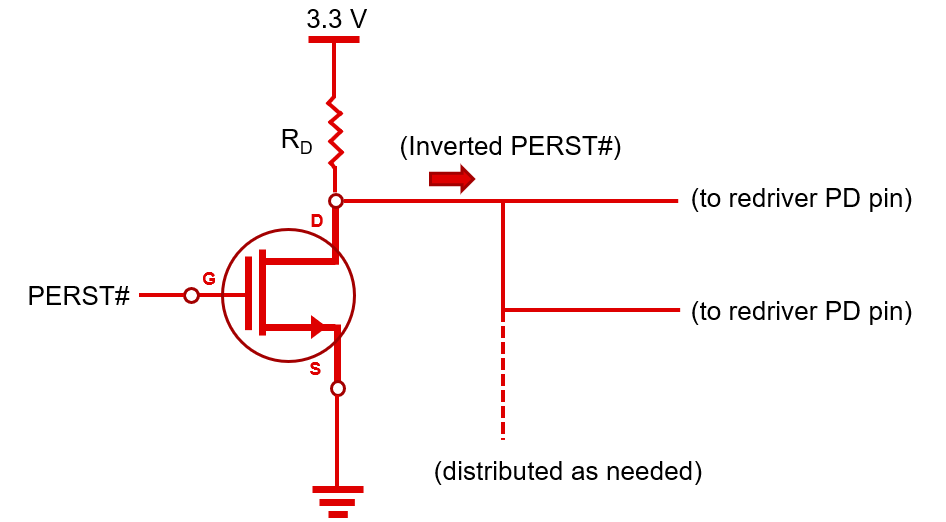
In typical applications, PERST# is routed from the root complex to the endpoint. Branching it to an inverter and routing the inverted signal to a redriver pin or multiple redriver pins is usually not an inconvenience to the board layout. The inverter implementation is left to the designer's discretion, but a basic MOSFET inverter or an inverter IC can both be suitable. Ensure that the input and output voltages of the inverter implementation are compatible with the PERST# signal and the PD pin. Figure 4-2 shows an example of how PERST# can be inverted and distributed to redriver PD pins.
 Figure 4-2 Inverted PERST# Distribution Example to Redriver PD Pins
An additional benefit of this PD configuration scheme happens during the initial system power-up: because PERST# initially stays low, the redriver can be held in reset until the PERST# transition triggers it to begin RX detection synchronously with the other system elements. If PD is simply pulled low with a hardwired connection to ground, the redriver begins RX detection as soon as its comparatively fast power-on sequence completes. At this early point in time prior to the PERST# transition, certain PCIe endpoints may present erroneous or unsynchronized terminations before their own power-up sequences are fully completed, which the redriver can then detect and act on. Leading to a similar situation as the warm reset case, the root complex can see erroneous early terminations from the redriver and the chance of linkup problems is higher.
In cases where the PD pins are intended to be controlled with other signals in addition to the inverted PERST#, such as a connection to PRSNT# for hot-plug functionality, it is safer to arbitrate the multiple control signals with a logic OR gate, as shown in the example of Figure 4-3. Without detailed knowledge of the mechanisms generating each control signal, it is difficult to predict if connecting them to the same node at the PD pins can operate normally, or if there can be conflicts resulting in incorrect voltages and other problems.
 Figure 4-3 PD Control Logic Example with Two Input Signals