SNOAA18A January 2019 – September 2024 TLV3011 , TLV3011-Q1 , TLV3011B , TLV3011B-Q1 , TLV3012-Q1 , TLV3012B , TLV3012B-Q1 , TLV4021 , TLV4041
Design Goals
| Battery Voltage Levels (VBAT) | Comparator Output Status (OUT) | ||
|---|---|---|---|
| Undervoltage (VLOW) | Start-Up Operating Voltage (VHIGH) | Low Battery | Normal Operation |
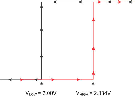
| < 2.000V | > 2.034V | VOL < 0.4V | VOH = VPU = 1.8V |
Design Description
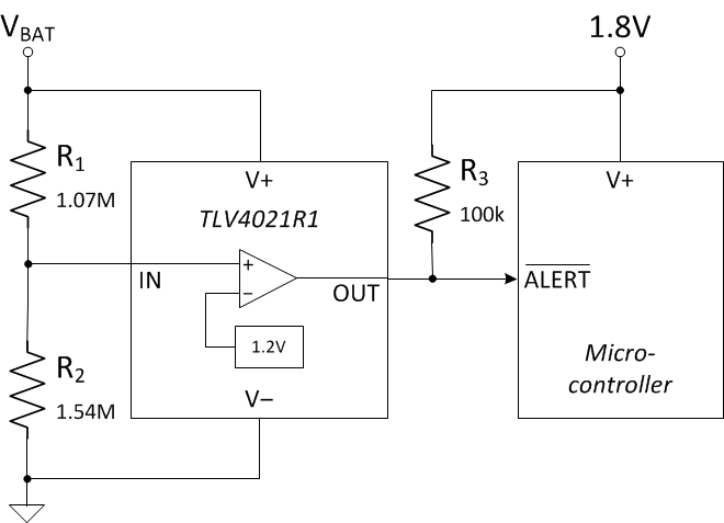
This undervoltage, protection circuit uses one comparator with a precision, integrated reference to create an alert signal at the comparator output (OUT) if the battery voltage sags below 2.0V. The undervoltage alert in this implementation is ACTIVE LOW. So when the battery voltage drops below 2.0V, the comparator output goes low, providing as an alert signal to whatever device is monitoring the output. Hysteresis is integrated in the comparator such that the comparator output will return to a logic high state when the battery voltage rises above 2.034V. This circuit utilizes an open-drain output comparator in order to level shift the output high logic level for controlling a digital logic input pin. For applications needing to drive the gate of a MOSFET switch, a comparator with a push-pull output is preferred.

Design Notes
- Select a comparator with a precision, integrated reference.
- Select a comparator with an open-drain output stage for level-shifting.
- Select values for the resistor divider so the critical undervoltage level occurs when the input to the comparator (IN) reaches the comparator's negative-going input threshold voltage (VIT-).
Design Steps
- Calculate the resistor divider
ratio needed so the input to the comparator crosses VIT- when
VBAT sags to the target undervoltage level (VLOW) of
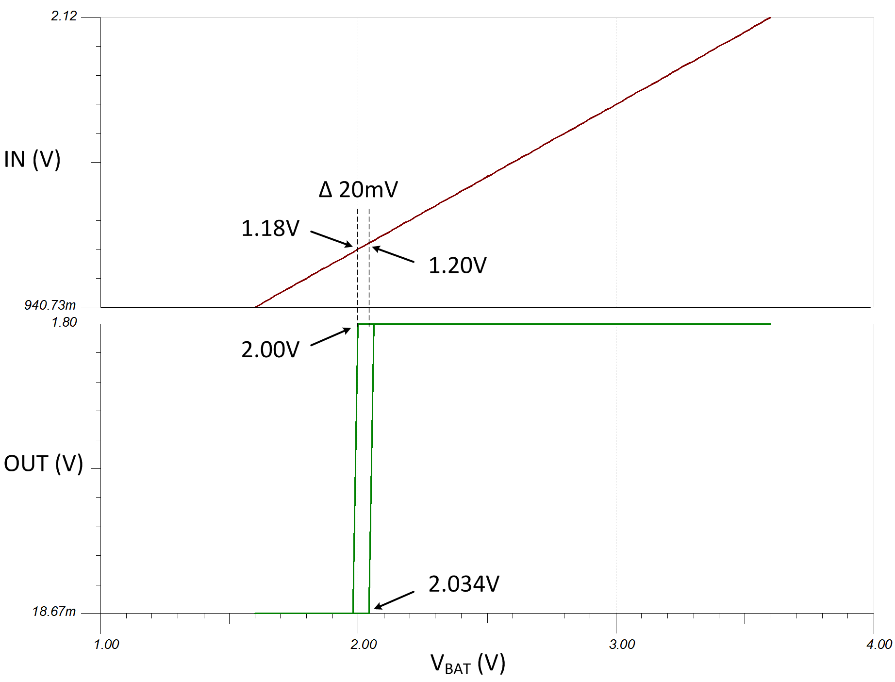
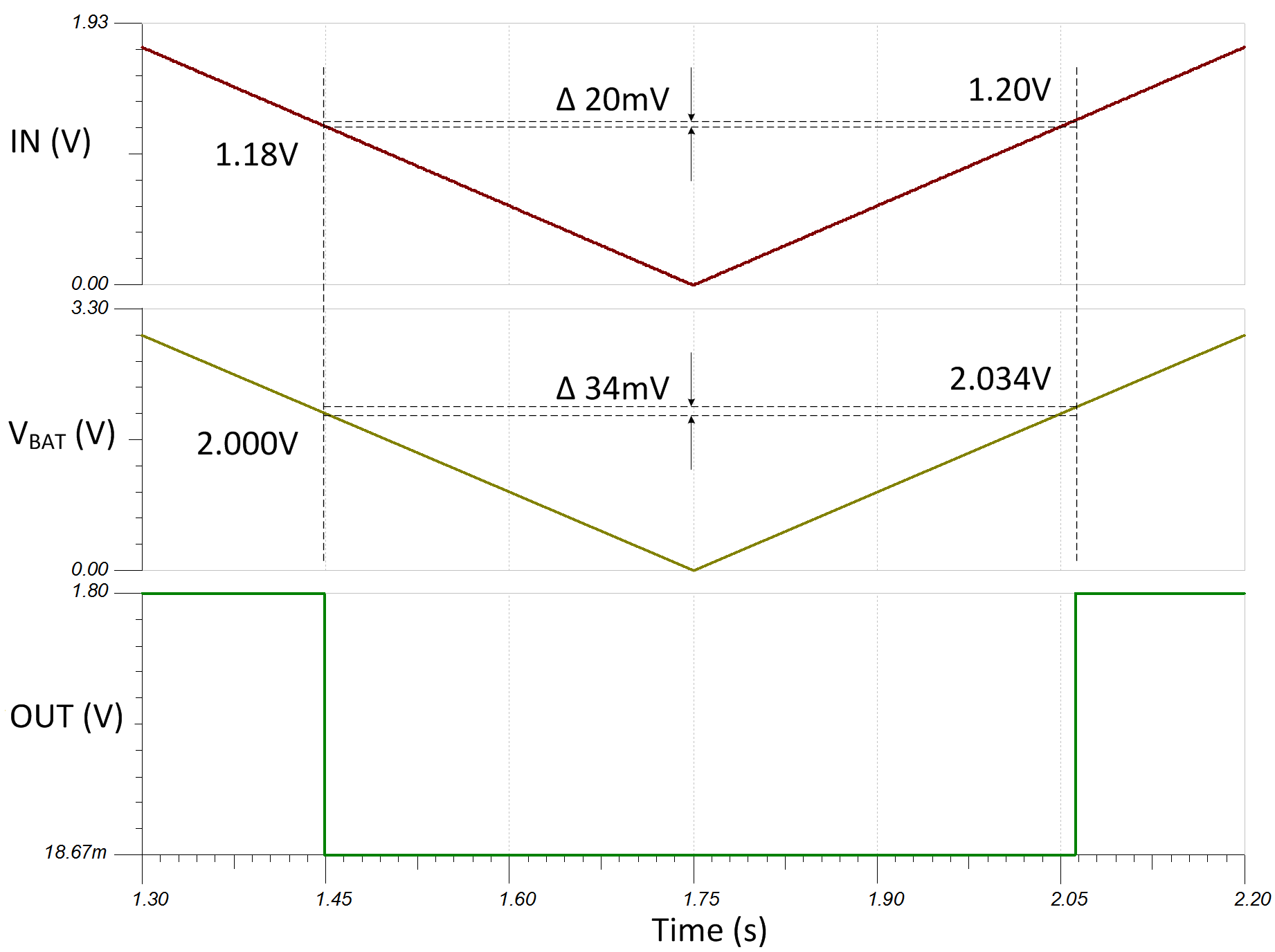
2.0V. VIT- from the TLV4021R1 data sheet is 1.18V.
- Confirm that the value of
VLOW, the voltage level where the undervoltage alert signal is
asserted, is 2.0V.
- Select values for R1 and
R2 that yield the resistor divider ratio of 0.59 by using the
following equation or using the online tool Voltage Divider Calculator.
If using the following equation, choose a value for R2 in the Mega-ohm range and calculate for R1. In this example, a value of 1.54 M was chosen for R2. - Verify that the current through the resistor divider is at least 100 times higher than the input bias current of the comparator. The resistors can have high values to minimize power consumption in the circuit without adding significant error to the resistor divider.
- Calculate VHIGH, the
battery voltage where the undervoltage alert signal is de-asserted (returns to a
logic high value). When the battery voltage reduces below the 2.0V level or is
ramping up at initial start-up, the comparator input needs to exceed
(VIT+), the positive-going input threshold voltage for the output
to return to a logic high. VIT+ from the TLV4021R1 data sheet is
1.20V.

Design Simulations
DC Simulation Results

Transient Simulation Results

References
Texas Instruments, High-Side Current Sensing with Comparator Circuit, analog engineer's circuit
Design Featured Comparator
| TLV4021R1 | |
|---|---|
| VS | 1.6V to 5.5V |
| VinCM | Rail-to-rail |
| VOUT | Open Drain |
| Integrated Reference | 1.2V ±1% over temperature |
| Hysteresis | 20mV |
| IQ | 2.5µA |
| tPD(HL) | 450ns |
| TLV4021R1 | |
Design Alternate Comparator