SNVA940 November 2021 LM5157 , LM5157-Q1 , LM51571-Q1 , LM5158 , LM5158-Q1 , LM51581 , LM51581-Q1
- Trademarks
- 1LM5157 Boost Design Example
-
2Calculations and Component Selection
- 2.1 Switching Frequency
- 2.2 Inductor Calculation
- 2.3 Slope Compensation Check
- 2.4 Inductor Selection
- 2.5 Diode Selection
- 2.6 Output Capacitor Selection
- 2.7 Input Capacitor Selection
- 2.8 UVLO Resistor Selection
- 2.9 Soft-Start Capacitor Selection
- 2.10 Feedback Resistor Selection
- 2.11 Control Loop Compensation
- 2.12 Power Loss and Efficiency Estimation
- 3Implementation Results
- 4Small Signal Frequency Analysis
2.11 Control Loop Compensation
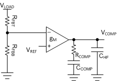
One benefit of the peak current mode control is the easier compensation design compared with that of the voltage mode control. A simple two-pole (one at origin), single zero network is adequate. A type II compensation network is implemented as shown in Figure 2-1, which provides a programmable zero and a pole. The following section introduces a general technique to set the crossover frequency and place the pole and zero of the error amplifier to achieve a stable system in the CCM boost. The detailed models of the control loop are presented in Section 4.
 Figure 2-1 Type II Compensation Network