SNVU770 June 2021 LM5157 , LM5157-Q1 , LM51571-Q1
6.5 Dynamic Responses
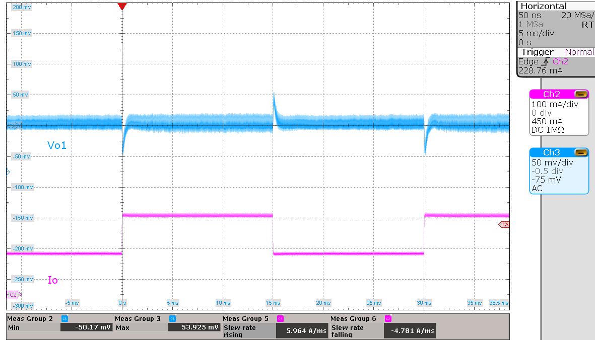 Figure 6-19 Vo1 Response Under Step
Load Between 125 mA and 250 mA, VIN = 12 V, Io2–4 = 10%
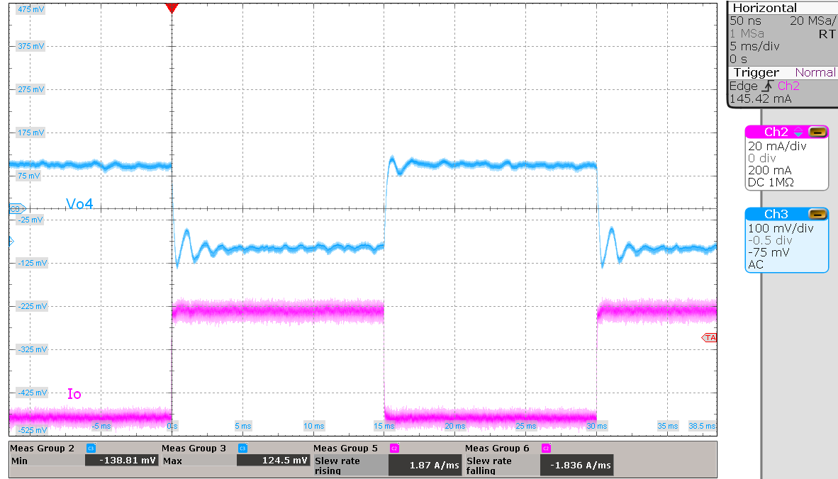 Figure 6-21 Vo4 Response Under Step
Load Between 100 mA and 150 mA, VIN = 12 V, Io1–3 = 10%
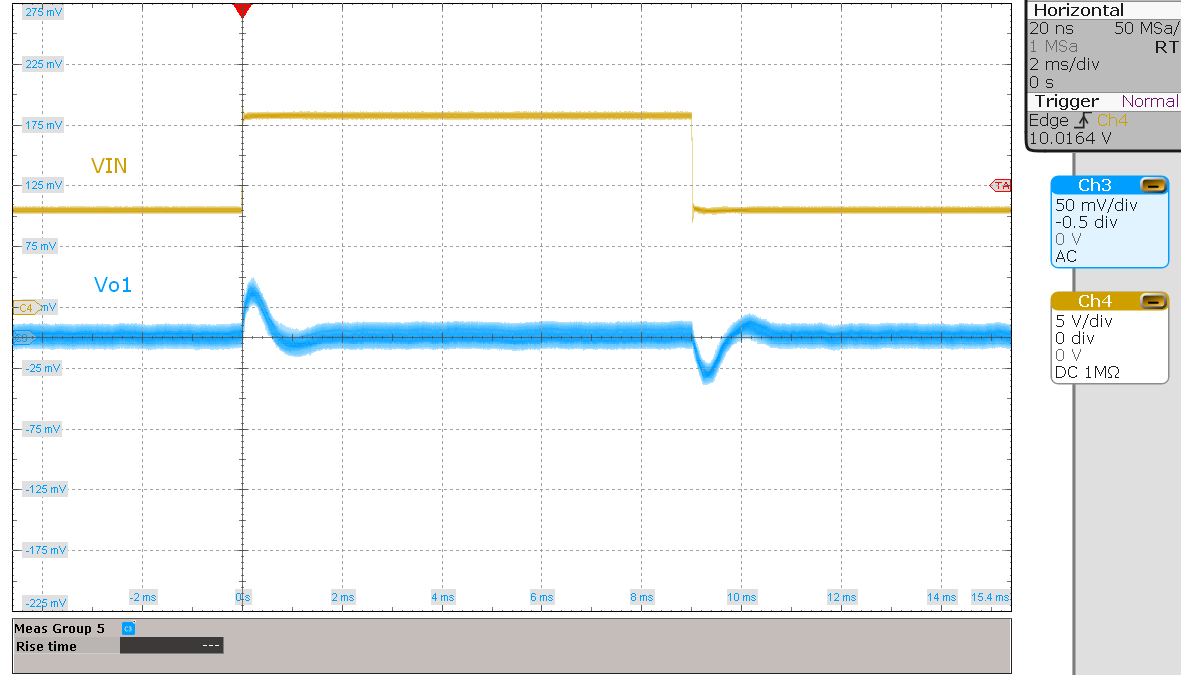 Figure 6-23 Vo1 Response Under Input
Change From 16 V to 8 V, 10% Load
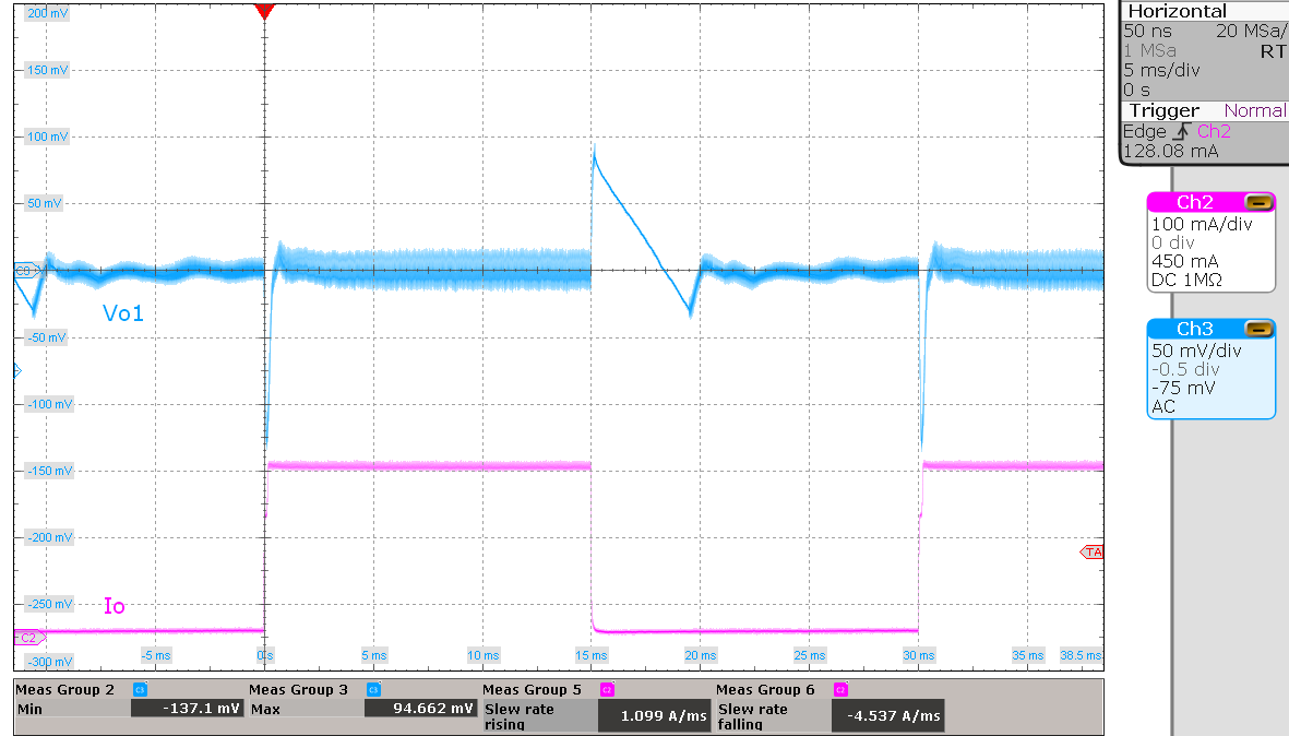 Figure 6-20 Vo1 Response Under Step
Load Between 1 mA to 250 mA, VIN = 12 V, Io2–4 = 10%
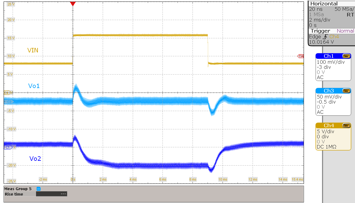 Figure 6-22 Vo1 Response Under Input
Change From 8 V to 16 V, 10% Load