SPRACW9A June 2021 – March 2023 F29H850TU , F29H850TU , F29H859TU-Q1 , F29H859TU-Q1 , TMS320F2800132 , TMS320F2800132 , TMS320F2800133 , TMS320F2800133 , TMS320F2800135 , TMS320F2800135 , TMS320F2800137 , TMS320F2800137 , TMS320F2800152-Q1 , TMS320F2800152-Q1 , TMS320F2800153-Q1 , TMS320F2800153-Q1 , TMS320F2800154-Q1 , TMS320F2800154-Q1 , TMS320F2800155 , TMS320F2800155 , TMS320F2800155-Q1 , TMS320F2800155-Q1 , TMS320F2800156-Q1 , TMS320F2800156-Q1 , TMS320F2800157 , TMS320F2800157 , TMS320F2800157-Q1 , TMS320F2800157-Q1 , TMS320F280021 , TMS320F280021 , TMS320F280021-Q1 , TMS320F280021-Q1 , TMS320F280023 , TMS320F280023 , TMS320F280023-Q1 , TMS320F280023-Q1 , TMS320F280023C , TMS320F280023C , TMS320F280025 , TMS320F280025 , TMS320F280025-Q1 , TMS320F280025-Q1 , TMS320F280025C , TMS320F280025C , TMS320F280025C-Q1 , TMS320F280025C-Q1 , TMS320F280033 , TMS320F280033 , TMS320F280034 , TMS320F280034 , TMS320F280034-Q1 , TMS320F280034-Q1 , TMS320F280036-Q1 , TMS320F280036-Q1 , TMS320F280036C-Q1 , TMS320F280036C-Q1 , TMS320F280037 , TMS320F280037 , TMS320F280037-Q1 , TMS320F280037-Q1 , TMS320F280037C , TMS320F280037C , TMS320F280037C-Q1 , TMS320F280037C-Q1 , TMS320F280038-Q1 , TMS320F280038-Q1 , TMS320F280038C-Q1 , TMS320F280038C-Q1 , TMS320F280039 , TMS320F280039 , TMS320F280039-Q1 , TMS320F280039-Q1 , TMS320F280039C , TMS320F280039C , TMS320F280039C-Q1 , TMS320F280039C-Q1 , TMS320F280040-Q1 , TMS320F280040-Q1 , TMS320F280040C-Q1 , TMS320F280040C-Q1 , TMS320F280041 , TMS320F280041 , TMS320F280041-Q1 , TMS320F280041-Q1 , TMS320F280041C , TMS320F280041C , TMS320F280041C-Q1 , TMS320F280041C-Q1 , TMS320F280045 , TMS320F280045 , TMS320F280048-Q1 , TMS320F280048-Q1 , TMS320F280048C-Q1 , TMS320F280048C-Q1 , TMS320F280049 , TMS320F280049 , TMS320F280049-Q1 , TMS320F280049-Q1 , TMS320F280049C , TMS320F280049C , TMS320F280049C-Q1 , TMS320F280049C-Q1 , TMS320F28075 , TMS320F28075 , TMS320F28075-Q1 , TMS320F28075-Q1 , TMS320F28076 , TMS320F28076 , TMS320F28374D , TMS320F28374D , TMS320F28374S , TMS320F28374S , TMS320F28375D , TMS320F28375D , TMS320F28375S , TMS320F28375S , TMS320F28375S-Q1 , TMS320F28375S-Q1 , TMS320F28376D , TMS320F28376D , TMS320F28376S , TMS320F28376S , TMS320F28377D , TMS320F28377D , TMS320F28377D-EP , TMS320F28377D-EP , TMS320F28377D-Q1 , TMS320F28377D-Q1 , TMS320F28377S , TMS320F28377S , TMS320F28377S-Q1 , TMS320F28377S-Q1 , TMS320F28378D , TMS320F28378D , TMS320F28378S , TMS320F28378S , TMS320F28379D , TMS320F28379D , TMS320F28379D-Q1 , TMS320F28379D-Q1 , TMS320F28379S , TMS320F28379S , TMS320F28384D , TMS320F28384D , TMS320F28384D-Q1 , TMS320F28384D-Q1 , TMS320F28384S , TMS320F28384S , TMS320F28384S-Q1 , TMS320F28384S-Q1 , TMS320F28386D , TMS320F28386D , TMS320F28386D-Q1 , TMS320F28386D-Q1 , TMS320F28386S , TMS320F28386S , TMS320F28386S-Q1 , TMS320F28386S-Q1 , TMS320F28388D , TMS320F28388D , TMS320F28388S , TMS320F28388S , TMS320F28P650DH , TMS320F28P650DH , TMS320F28P650DK , TMS320F28P650DK , TMS320F28P650SH , TMS320F28P650SH , TMS320F28P650SK , TMS320F28P650SK , TMS320F28P659DH-Q1 , TMS320F28P659DH-Q1 , TMS320F28P659DK-Q1 , TMS320F28P659DK-Q1 , TMS320F28P659SH-Q1 , TMS320F28P659SH-Q1
- Abstract
- Trademarks
-
1Introduction
- 1.1 Memory Cross-Talk Challenges
- 1.2
Resources for Signal Conditioning Circuit
Design
- 1.2.1 TI Precision Labs - SAR ADC Input Driver Design Series
- 1.2.2 Analog Engineer's Calculator
- 1.2.3 Related Application Reports
- 1.2.4 TINA-TI SPICE-Based Analog Simulation Program
- 1.2.5 PSPICE for TI
- 1.2.6 ADC Input Circuit Evaluation for C2000 MCUs
- 1.2.7 Charge-Sharing Driving Circuits for C2000 ADCs
- 2Review of ADC Input Settling
- 3Problem Statement
- 4Dedicated ADC Sampling
- 5Pre-Sampling VREFLO
- 6Summary
- 7References
- 8Revision History
4.1 Dedicated ADC Concept
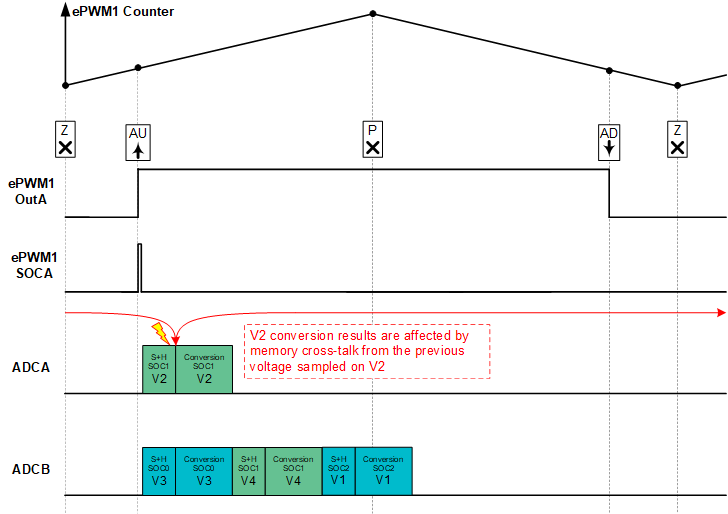
In the system presented in Section 3.1, two ADCs are used to sample four voltages, only one of which is specified to have poor input settling performance (voltage V2). Allocating two signals to each of the two ADCs results in the shortest overall latency to process the four voltages. However, if the sampling scheme is rearranged as shown in Figure 4-1, then the signal with poor settling performance (voltage V2) receives a dedicated ADC.
 Figure 4-1 Timings for
Dedicated ADC Method
Figure 4-1 Timings for
Dedicated ADC MethodThe main benefit of isolating the affected signal onto a single ADC is that the memory cross-talk error now originates from the previously sampled value of the same signal. If the signal is not moving very fast, the S+H circuit will start with a value close to the current input voltage. This greatly reduces the distance the input has to settle, resulting in acceptable settling performance. However, if the input experiences a large step in the input voltage, it may take several samples for the ADC to catch up with the new value on the input. Thus, a dedicated ADC strategy is generally more appropriate for slow moving or DC input signals. However, even in the case of faster signals, the memory cross-talk effect at least becomes systematic, which is usually an improvement compared with a memory error coupling into the signal in question from an unrelated signal.
Of course, dedicating an ADC to sample a single input signal results in increased latency in processing the remaining signals in the application. For instance, after re-arranging the signals as shown in Figure 4-1, the latency to produce the final ADC result has increased by 50%! (assuming all conversions are configured to take the ADC equal amounts of time to process).