SPRACY9 March 2023 F29H850TU , F29H850TU , F29H859TU-Q1 , F29H859TU-Q1 , TMS320F2800132 , TMS320F2800132 , TMS320F2800133 , TMS320F2800133 , TMS320F2800135 , TMS320F2800135 , TMS320F2800137 , TMS320F2800137 , TMS320F2800152-Q1 , TMS320F2800152-Q1 , TMS320F2800153-Q1 , TMS320F2800153-Q1 , TMS320F2800154-Q1 , TMS320F2800154-Q1 , TMS320F2800155 , TMS320F2800155 , TMS320F2800155-Q1 , TMS320F2800155-Q1 , TMS320F2800156-Q1 , TMS320F2800156-Q1 , TMS320F2800157 , TMS320F2800157 , TMS320F2800157-Q1 , TMS320F2800157-Q1 , TMS320F280021 , TMS320F280021 , TMS320F280021-Q1 , TMS320F280021-Q1 , TMS320F280023 , TMS320F280023 , TMS320F280023-Q1 , TMS320F280023-Q1 , TMS320F280023C , TMS320F280023C , TMS320F280025 , TMS320F280025 , TMS320F280025-Q1 , TMS320F280025-Q1 , TMS320F280025C , TMS320F280025C , TMS320F280025C-Q1 , TMS320F280025C-Q1 , TMS320F280033 , TMS320F280033 , TMS320F280034 , TMS320F280034 , TMS320F280034-Q1 , TMS320F280034-Q1 , TMS320F280036-Q1 , TMS320F280036-Q1 , TMS320F280036C-Q1 , TMS320F280036C-Q1 , TMS320F280037 , TMS320F280037 , TMS320F280037-Q1 , TMS320F280037-Q1 , TMS320F280037C , TMS320F280037C , TMS320F280037C-Q1 , TMS320F280037C-Q1 , TMS320F280038-Q1 , TMS320F280038-Q1 , TMS320F280038C-Q1 , TMS320F280038C-Q1 , TMS320F280039 , TMS320F280039 , TMS320F280039-Q1 , TMS320F280039-Q1 , TMS320F280039C , TMS320F280039C , TMS320F280039C-Q1 , TMS320F280039C-Q1 , TMS320F280040-Q1 , TMS320F280040-Q1 , TMS320F280040C-Q1 , TMS320F280040C-Q1 , TMS320F280041 , TMS320F280041 , TMS320F280041-Q1 , TMS320F280041-Q1 , TMS320F280041C , TMS320F280041C , TMS320F280041C-Q1 , TMS320F280041C-Q1 , TMS320F280045 , TMS320F280045 , TMS320F280048-Q1 , TMS320F280048-Q1 , TMS320F280048C-Q1 , TMS320F280048C-Q1 , TMS320F280049 , TMS320F280049 , TMS320F280049-Q1 , TMS320F280049-Q1 , TMS320F280049C , TMS320F280049C , TMS320F280049C-Q1 , TMS320F280049C-Q1 , TMS320F28075 , TMS320F28075 , TMS320F28075-Q1 , TMS320F28075-Q1 , TMS320F28076 , TMS320F28076 , TMS320F28374D , TMS320F28374D , TMS320F28374S , TMS320F28374S , TMS320F28375D , TMS320F28375D , TMS320F28375S , TMS320F28375S , TMS320F28375S-Q1 , TMS320F28375S-Q1 , TMS320F28376D , TMS320F28376D , TMS320F28376S , TMS320F28376S , TMS320F28377D , TMS320F28377D , TMS320F28377D-EP , TMS320F28377D-EP , TMS320F28377D-Q1 , TMS320F28377D-Q1 , TMS320F28377S , TMS320F28377S , TMS320F28377S-Q1 , TMS320F28377S-Q1 , TMS320F28378D , TMS320F28378D , TMS320F28378S , TMS320F28378S , TMS320F28379D , TMS320F28379D , TMS320F28379D-Q1 , TMS320F28379D-Q1 , TMS320F28379S , TMS320F28379S , TMS320F28384D , TMS320F28384D , TMS320F28384D-Q1 , TMS320F28384D-Q1 , TMS320F28384S , TMS320F28384S , TMS320F28384S-Q1 , TMS320F28384S-Q1 , TMS320F28386D , TMS320F28386D , TMS320F28386D-Q1 , TMS320F28386D-Q1 , TMS320F28386S , TMS320F28386S , TMS320F28386S-Q1 , TMS320F28386S-Q1 , TMS320F28388D , TMS320F28388D , TMS320F28388S , TMS320F28388S , TMS320F28P650DH , TMS320F28P650DH , TMS320F28P650DK , TMS320F28P650DK , TMS320F28P650SH , TMS320F28P650SH , TMS320F28P650SK , TMS320F28P650SK , TMS320F28P659DH-Q1 , TMS320F28P659DH-Q1 , TMS320F28P659DK-Q1 , TMS320F28P659DK-Q1 , TMS320F28P659SH-Q1 , TMS320F28P659SH-Q1
- Abstract
- Trademarks
- 1Introduction
- 2Input Settling Design Steps
-
3Example Circuit Design
- 3.1 Select the ADC
- 3.2 Find the Minimum Op-Amp Bandwidth and RC Filter Ranges
- 3.3 Verify the Op-Amp Model
- 3.4 Build the ADC Input Model
- 3.5 Bias Point Analysis to Determine Voa_ss
- 3.6 Transient Analysis to Determine Voa_ss
- 3.7 Perform Initial Transient Analysis
- 3.8 Iterative Approach to Refine RC Filter Values
- 3.9 Perform Final Transient Analysis
- 3.10 Perform Final Transient Analysis
- 3.11 Further Refinement
- 3.12 Further Simulations
- 3.13 Completed Worksheet
- 4Working With Existing Circuits or Additional Constraints
- 5Summary
- 6References
3.8 Iterative Approach to Refine RC Filter Values
Now that the basic simulation has shown that the simulation is fundamentally working, sweeps can be performed to refine the Rs component selection.
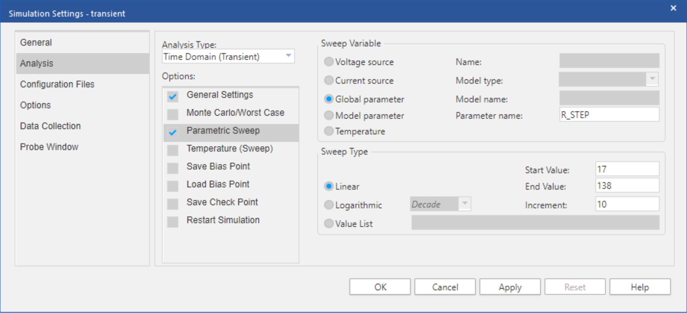
To perform a sweep, open the transient simulation profile and enable the Parametric Sweep option. In the Parametric Sweep settings, choose the global parameter R_STEP as the sweep variable. Then choose a linear sweep type with a start value of 17 Ω, an end value of 138 Ω, and an increment of 10 Ω as shown in Figure 3-12.
 Figure 3-12 F280049 Example Parametric
Sweep Settings
Figure 3-12 F280049 Example Parametric
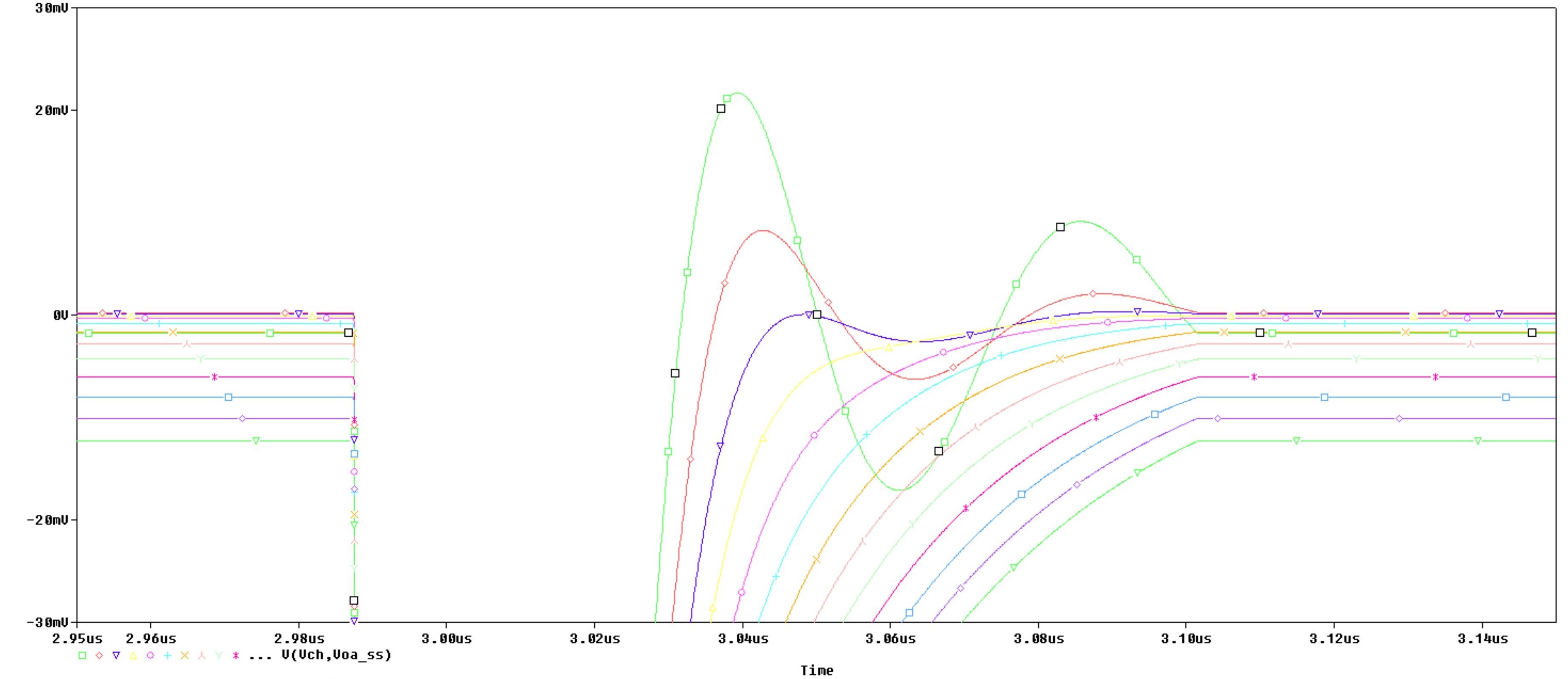
Sweep SettingsAfter performing the analysis, delete all outputs other than Verror and set Verror range to -30 mV to +30 mV. Additionally, limit the waveform to +2.95 µs to +3.15 µs to better observe the settling. Alternatively, go to Window ➔ Display Control... using the menu in the upper left of the PSpice for TI simulation window to access a list of preset display configurations provided by TI. Restore the Sweep Results display configuration. Note that these preset display configurations are only available in the PSpice for TI projects bundled with this application report. Figure 3-13 shows the output of the transient simulation with a sweep of Rs.
From this output, it can be concluded:
- Higher resistance values in the Rs range do not provide quick enough settling. For instance, 107 Ω only settles to 6.1 mV in the allocated S+H time while the settling target is 366 µV
-
A good range for further investigation would be 20 Ω to 60 Ω. Determining the optimal value of Rs requires further analysis, which may include additional simulations
 Figure 3-13 F280049 Example Rs
Initial Sweep Results
Figure 3-13 F280049 Example Rs
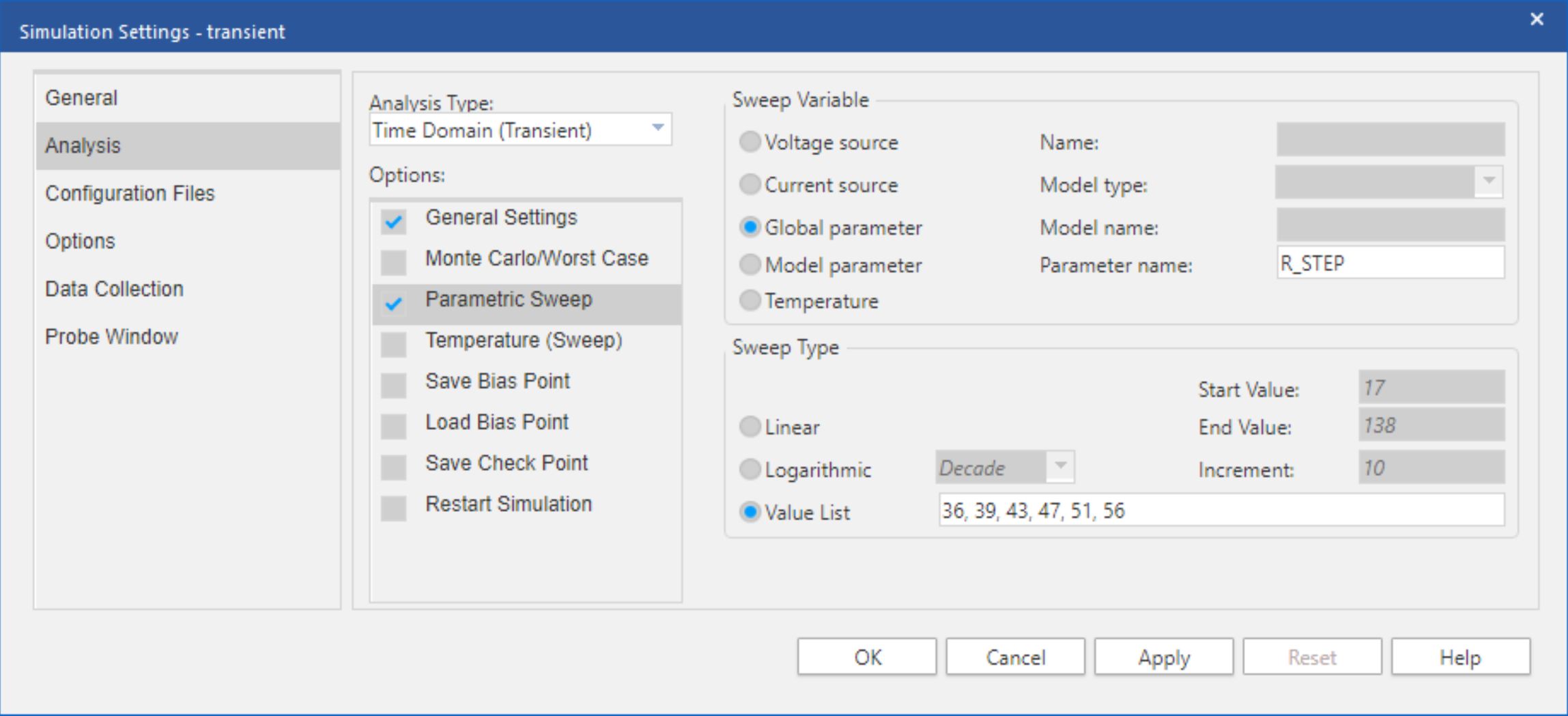
Initial Sweep ResultsBased on the initial sweep results, it may already be possible to identify one or more values of Rs that provide adequate settling. If desired, the Rs component selection can be further refined by iteratively narrowing the linear sweep range. A value list sweep may also be performed to test values of Rs that are not linearly spaced. An example simulation profile for a value list sweep is shown in Figure 3-14.
 Figure 3-14 F280049 Example Parametric
Sweep Settings
Figure 3-14 F280049 Example Parametric
Sweep SettingsThus, a final value of Rs can be selected that provides adequate settling. With enough iterations, the final value of Rs can be made optimal. However, Section 3.9 introduces an alternative method to better select the optimal value of Rs using the Performance Analysis tool.