SPRADM8 November 2024 AM2612 , AM2631 , AM2631-Q1 , AM2632 , AM2632-Q1 , AM2634 , AM2634-Q1 , AM263P4 , AM263P4-Q1
As cybersecurity regulations are becoming widely enforced to make sure that the devices in Automotive and Industrial domains are safe from malicious attacks. The TI SoCs are being widely used in these domain. The TI AM26x SoCs is a real time capable device with multitude of features like Real time ARM R cores, advance sensing, precise control, gigabit connectivity and dedicated components that enables design of systems with cyber security and functional safety requirements. In this document we can be looking at secure boot enhancements and performance benchmarks for AM26x SoC family.
Introduction
The advantage an external flash device offers is flexible NVM memory size for storing application software without upgrading or changing the existing SoC, when challenged with memory constraints. On the flip side, if proper security measures are not in place,then an unauthorized program can be loaded into the memory. The unauthorized program can render the system to be inoperable, expose sensitive and confidential data to the malicious agent, and in cases, can have life threatening consequences, damages to reputation, and legal liabilities.
AM26x (AM263x and AM263Px) device family supports securely booting the user code without compromising on the authenticity and confidentiality of user information like code, data, keys, and so on. AM26x microcontroller family support interfaces like OSPI and QSPI which allow integration of external flash devices and also providing secure boot feature. Thus enabling the user with the flexibility of external flash technology while maintaining the security of the system.
Cryptographic Strengths of AM26 Secure Boot include:
- RSA-PKCS1-v1_5 and SHA512 digest is used for verification of the certificate
- SHA512 is used to maintain the integrity of the bootloader Image.
- AES-CBC-256 is used to decrypt the image to maintain the confidentiality of the image.
Fast Boot Techniques
The following sections include information about different boot optimization techniques used to improve boot time performance.
Flash Clock, Configuration, and DMA integration
AM26x device family does not have an internal non-volatile memory for code execution and relies heavily on internal volatile memories (TCM and SRAM). Like many other advance SOCs, AM26x devices also have multi stage boot architecture. During the ROM bootloader(RBL) the copies the Secondary bootloader(SBL) image from external flash (over SPI) into the internal memory. In SPI protocol, the data speed (bps) is directly proportional to the frequency (Hz) at which SPI peripheral is clocked. As per JEDEC xSPI standard configuring the OSPI controller to support higher modes enables faster data transfers. Hence, a higher SPI clock and higher configuration can lead to better performance.
| AM263x | AM263Px | |
|---|---|---|
| Maximum Flash Clock | 80MHz | 133MHz |
| Maximum configuration supported | 1s-1s-4s | 8d-8d-8d |
| DMA integration with flash controller | YES | YES |
Optimized OSPI PHY Tuning (valid only for AM263Px)
The OSPI controller on AM263Px SOC integrates a dedicated PHY module which enables flexible and energy efficient transfers. This gives us ability to the flash clock to be used over 50MHz in Single Transfer Rate (STR) mode and 25MHz in Dual Transfer Rate (DTR) mode. This PHY requires software calibration across all the valid values before configuring the PHY_CONFIG_TX_DLL_DELAY_FLD and PHY_CONFIG_RX_DLL_DELAY_FLD in OSPI_PHY_CONFIGURATION_REG. Thus optimizing the software algorithm to span over limited values to complete the calibration in less than 2.5ms.
Refer to AM263Px TRM (13.3.3.6) to learn more about OSPI Controller and PHY module. Application Note on Optimized PHY Tuning here.
Image Format (MCELF)
Multicore ELF, or MCELF is an ELF (Executable and Linkable format) standard based application image format, unlike the previously adopted proprietary RPRC format. An executable file using the ELF file format consists of an ELF header, followed by a program header table or a section header table, or both. The program header table and the section header table's offset in the file are defined in the ELF header. The two tables describe the rest of the particularities of the file. The table summarizes the advantage of MCELF format vs RPRC format.
| Feature | RPRC | Multicore ELF |
|---|---|---|
| Image generation Tools | Custom | Open source |
| Readable by standard ELF tools | No | Yes |
| Customizable meta data | No | Yes |
| Customizable data segment sizes | No | Yes |
| XIP | Yes | Yes |
| Secure boot time | Slow | Fast |
Streaming Support of Secure Boot
Verification of images directly in the flash memory induces a bottleneck due to limited flash clock, and a lack of scratchpad memory leads to Secure Boot images not being able be copied into the memory for the verification. Verification of secure boot images into the external flash also adds a lot of limitations in security by risking the software to TOCTOU attacks. Hence, the streaming secure boot allows users to copy the image into the memory in the SBL and then issuing a call to the TIFS-MCU services to authenticate the image in the streaming mode. This utilizes the execution memory for placement and authentication which in-turn enhances the authentication speed.
Crypto DMA
The DTHE (Data Transform and Hashing Engine) is a wrapper on top of the Crypto IP which is integrated with AM26 device. The DTHE supports EDMA (Enhanced DMA) integration to offload burst data transfers. Enhanced DMA can be programmed to be event-triggered and can automatically transfer the data based on the configured burst size. This allows the Crypto IP events to be configured as EDMA source events allowing complete CPU offload.
| Data | Without DMA (in Mbps) | With DMA (in Mbps) | Improvement |
|---|---|---|---|
| SHA512 | |||
| 4KB | 250.41 | 679.58 | 2.7x |
| 16KB | 265.65 | 1024.60 | 3.85x |
| AES-CBC-256 | |||
| 4KB | 93.61 | 239.30 | 2.55x |
| 16KB | 94.81 | 301.54 | 3.18x |
The RSA signature verification are not impacted by the DMA integration in DTHE. For more information, read the PKE hardware integration in TIFS-MCU documentation.
Parallelization of Flash Usage With Secure Boot Services
Next avenue for optimization is in SBL, where the sequential flash reads were modified to do parallel reads. After adding parallelization in SBL to support parallel flash reads of (n+1) th sections while the TIFS-MCU is validating the (n)th sections. Further enhancements were achieved by adding the support for queuing of SIPC messages at HSM server and handling the same in order, for example, the support of sending non-blocking requests and handling of the multiple responses from the HSM on the client (SBL). Below is a visual representation of TIFS-MCU occupied while the SBL is reading from the Flash.
 Figure 1 Boot Parallelization
Secure Boot Benchmark
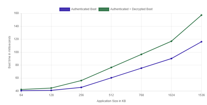
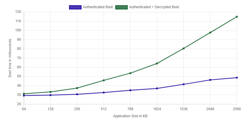
With the implementation of the previously mentioned techniques, significant increase in the boot time performance is shown and summarized in Table 4.
AM263x
- SBL size - 55KB. SBL is encrypted as well as authenticated.
- TIFS-MCU size - 70KB. TIFS-MCU is encrypted as well as authenticated.
| Application Size | Authentication Only | Encryption + Authentication Only |
|---|---|---|
| 64KB | 40.53ms | 43.40ms |
| 128KB | 41.05ms | 44.58ms |
| 256KB | 45.62ms | 56.18ms |
| 512KB | 60.45ms | 76.39ms |
| 1024KB | 90.16ms | 116.92ms |
 Figure 2 AM263x Boot Performance
AM263Px
- SBL size - 60KB. SBL is encrypted as well as authenticated.
- TIFS-MCU size - 61KB. TIFS-MCU is encrypted as well as authenticated.
| Application Size | Authentication Only | Encryption + Authentication Only |
|---|---|---|
| 1024KB | 37.11ms | 64.13ms |
| 512KB | 32.61ms | 45.85ms |
| 256KB | 30.74ms | 37.48ms |
| 128KB | 29.83ms | 33.31ms |
| 64KB | 29.35ms | 30.26ms |
 Figure 3 AM263Px Boot Performance
Conclusion
Secure boot has additional run time overhead due to authentication and image integrity verification. However, by employing the software design and hardware offload techniques there is a possibility to improve the secure boot time thus improving the over system performance. In automotive systems, the boot time goals are quite stringent while offering little compromise on the security of the system. The optimized secure boot methods for AM26x family SOC discussed in this paper is targeted to solve the same challenge while utilizing the efficient hardware architecture and software design.