SSZTD42 July 2024 TPSM81033 , TPSM82813 , TPSM82816 , TPSM828303 , TPSM82866A , TPSM82866C

Are you working to double the data rate of your next-generation optical module, but within the existing form factor and power budget? Or are you being asked to cram one more sensor into your machine vision system, but are already out of board space and dissipating too much power?
If you need something more in a power module besides just a small improvement over the previous generation, our new power modules leverage TI's new proprietary integrated-magnetic packaging (MagPack™) technology to increase power density, efficiency and thermal performance, offering ease of use and reducing electromagnetic interference (EMI) for industrial, enterprise and communications applications.
Here are four key benefits.
- Benefit No. 1: Higher power
density and smaller solution size
MagPack technology helps achieve a higher power density and smaller overall solution size. In fact, the 6A TPSM82866A, TPSM82866C and TPSM82816 all achieve a smaller size than any other 6A power module on the market.
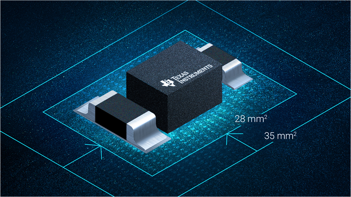
Power density is measured as output current per unit area in square millimeters. At 2.3mm by 3mm, the TPSM82866A and TPSM82866C both have an area of 6.9mm2. This leads to a power density per area of almost 1A/mm2 (0.87A/mm2, to be exact). To supply nearly 1A per 1mm2 of area is extraordinary, especially considering that an 0603 (imperial, or 1608 metric) component occupies 1.28mm2 of board space. The standard printed circuit board (PCB) design of the evaluation module (EVM), with easy design rules and large passive components, yields a total solution size of 28mm2 for a complete 6A power supply.
If you require additional features such as adjustable soft start, adjustable switching frequency, clock synchronization and adjustable control loop compensation, the TPSM82816 provides these in a slightly larger 2.5mm by 3mm package. The extra features require additional pins and passive components, which increases the total solution size to 46mm2. This is still very small for a 6A power supply and delivers 0.8A/mm2 of power density. Figure 1 and Figure 2 show the total solution sizes for both devices.
Figure 1 TPSM82866A and TPSM82866C total solution size of 28mm2
Figure 2 TPSM82816 total solution size of 46mm2
- Benefit
No. 2: High efficiency and good thermal performance
Immediately after shrinking the size and increasing the power density, it is essential to effectively remove heat from the smaller package and maintain reliable operation of the power module. The inductor used in MagPack technology is matched to the silicon die to reduce both DC and AC losses. Pairing these two circuit elements with a high-performance, high-conductivity MagPack package helps efficiently remove heat from the power module.
The silicon now has an optimized inductor and package delivering high efficiency and a low temperature rise. Figure 3 shows the efficiency of the TPSM82866A, while Figure 4 shows the safe operating area (SOA). Such a high SOA curve enables reliable operation at higher ambient temperatures and reduced derating for long-lifetime applications.
Figure 3 The TPSM82866A delivers high efficiency with MagPack technology
Figure 4 The TPSM82866A’s SOA curve enables operation at very high ambient temperatures
- Benefit
No. 3: Ease of use to enable faster time to market
Devices using MagPack technology integrate the inductor, which is usually the most difficult item to select and source in a power-supply design. It is also one of the most difficult items to place and route on the PCB, given its size, height and interference with other circuitry. Power modules that integrate the inductor eliminate these issues, and the inductor used in MagPack technology eases these challenges even more. MagPack technology provides high efficiency and great thermal performance, and it also alleviates another concern of all power-supply designs: EMI.
- Benefit No. 4: Reduced EMI
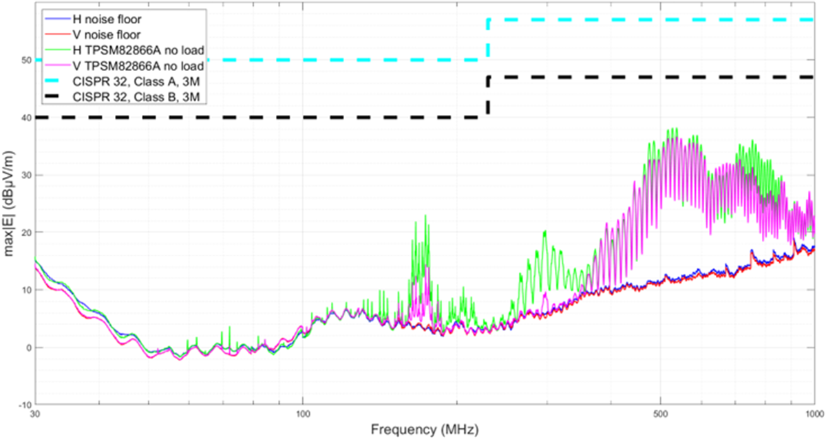
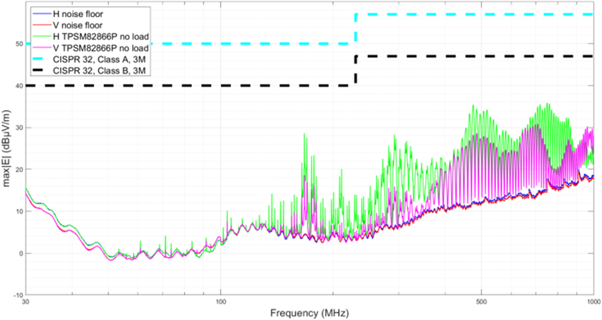
Power modules with MagPack technology are shielded. And this is not just a shielded inductor. The entire die, the inductor, the switching node – all are enclosed in a shielded package. Additionally, the size of power modules with MagPack technology and the optimized routing inside the package make for shorter, smaller routings of noisy signals, in both the power module and the system. Figure 5 and Figure 6 compare preliminary measured radiated emissions of the TPSM82866A without MagPack technology and with it. Peak emissions are reduced by about 2dB in the horizontal polarization and 8dB in the vertical polarization.
 Figure 5 Radiated emissions of the
TPSM82866A without MagPack technology
 Figure 6 Radiated emissions of the
TPSM82866A with MagPack technology
Conclusion
No matter what sort of power conversion system you are working on, it can be smaller and highly efficient, while being thermally capable and easy to use, with our new power modules that leverage MagPack technology. Imagine shrinking each of your point-of-load (POL) power supplies by 20% in size – what could you accomplish with that extra board space? Maybe it’s a higher data rate or channel count, or maybe you can add an extra feature or sensor to your product. MagPack technology delivers a better power module, which enables you to deliver a better product to your customers. What design challenges can power modules with MagPack technology enable you to solve?
MagPack Technology Power Modules
| Device | Input voltage range | Description | MagPack package | Evaluation Module |
|---|---|---|---|---|
| TPSM82866A | 2.4V to 5.5V | Industry’s smallest 6A step-down module with integrated inductor & 13 fixed VOUT options | 2.3mm-by-3mm | TPSM82866AA0PEVM |
| TPSM82866C | 2.4V to 5.5V | Industry’s smallest 6A step-down module with integrated inductor & I2C interface | 2.3mm-by-3mm | TPSM82866CA3PEVM |
| TPSM828303 | 2.25V to 5.5V | 3A, step-down module with integrated inductor & noise-filtering capacitors | 2.5mm-by-2.6mm | TPSM828303PEVM-058 |
| TPSM82816 | 2.7V to 6V | Industry’s smallest 6A step-down module with adjustable-frequency & synchronization | 2.5mm-by-3mm | TPSM82816PEVM-062 |
| TPSM82813 | 2.75V to 6V | 3A step-down module with adjustable-frequency & synchronization | 2.5mm-by-3mm | TPSM82813PEVM-062 |
| TPSM81033 | 1.8V to 5.5V | 5.5A valley current limit boost module with power good, output discharge & PFM/PWM control | 2.5mm-by-2.6mm | TPSM81033EVM-035 |
Additional resources
- Watch our training video, Achieve Small Size and Great Thermal Performance with DC/DC Power Modules.
- Learn more about our power modules portfolio.
- Register for our New Product Webinar on Aug. 8 to learn more about MagPack technology.
- See all MagPack technology devices
Trademarks
All trademarks are the property of their respective owners.