-
Design considerations of a 10kW single-phase string inverter based on TI GaN FETs
Design considerations of a 10kW single-phase string inverter based on TI GaN FETs
Riccardo Ruffo and Vedatroyee Ghosh
Energy sustainability and security concerns are accelerating demand for energy storage systems, particularly in residential solar installations. There are microinverters with integrated energy storage systems on the market with power as high as 2kW. When a system requires higher power, there are string inverters or hybrid string inverters that also have an energy storage system connected.
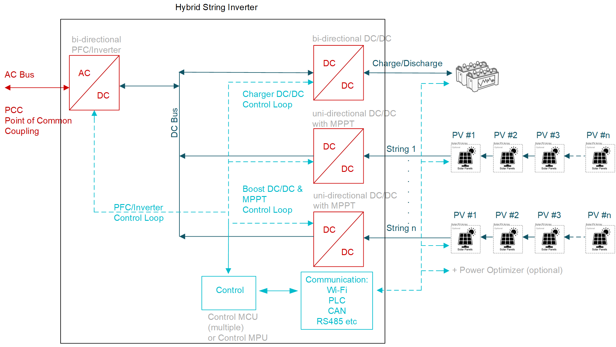
Figure 1 is a block diagram of a hybrid string inverter. A common regulated DC bus interconnects the fundamental blocks. A hybrid string inverter comprises these subblocks:
- A unidirectional DC/DC converter for performing maximum power-point tracking.
- A bidirectional DC/DC converter for charging and discharging the battery. The battery makes it possible to provide power at night or during an outage.
- A DC-to-AC converter, responsible for converting DC to AC power and maintaining low-current total harmonic distortion (THD).
- A microcontroller (MCU) to measure currents and voltages, control the power switches, perform insulation monitoring, detect string arching, and enable communication.
- A power optimizer for maximizing available power from a photovoltaic panel, independent of external variables such as irradiance and temperature.
 Figure 1 Schematic of a hybrid string
inverter tied to the grid
Figure 1 Schematic of a hybrid string
inverter tied to the gridIGBTs vs. GaN FETs
String inverters consist of power switches such as insulated gate bipolar transistors (IGBTs). This kind of power device has issues such as tail current and diode reverse recovery, which lead to high switching losses. Furthermore, these phenomena are affected by temperature, leading to higher power losses, especially for static-cooled solutions. Therefore, these power devices need to run at low frequencies, requiring bulkier passives and a bulkier heat sink. Typically, the switching frequency can range from 5kHz to 15kHz.
Wide-bandgap power switches such as gallium nitride (GaN) have no minority carrier phenomenon, thus enabling a reduction in switching losses. Decreased switching losses enable an increase in switching frequencies by maintaining the same system losses, therefore allowing a reduction in passive components. On average, the switching frequency increases by a factor of six.
This article proposes a 10kW string inverter based on GaN field-effect transistors (FETs). We will also explore the benefits of GaN and highlight the advantages of building such a system for residential solar applications.
Design considerations of a GaN based string inverter
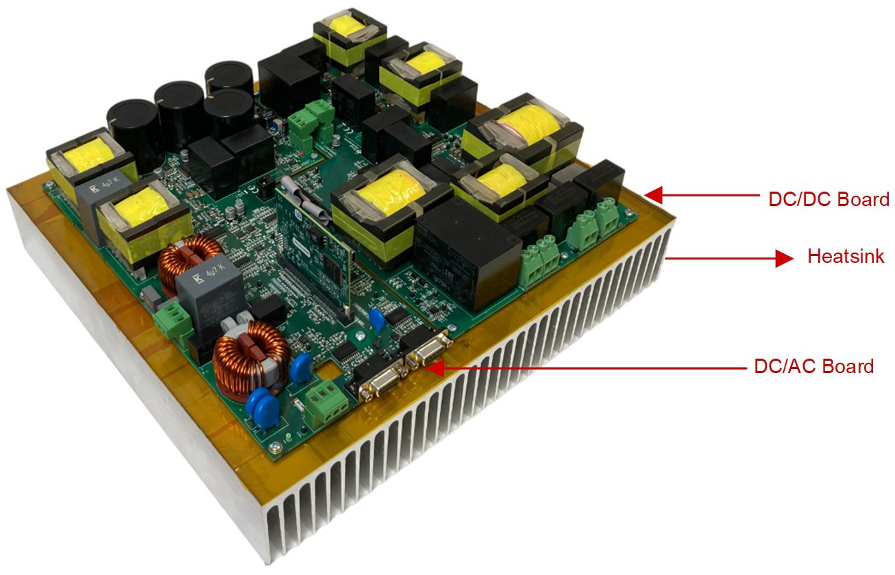
Figure 2 illustrates the 10kW, GaN-Based Single-Phase String Inverter with Battery Energy Storage System Reference Design, including all active and passive components.
 Figure 2 A 10kW single-phase reference
design based on GaN devices
Figure 2 A 10kW single-phase reference
design based on GaN devicesFigure 3 is a schematic representation of the converter.
 Figure 3 Single-phase string inverter
reference design block diagram
Figure 3 Single-phase string inverter
reference design block diagramThe reference design consists of four power-conversion systems operating at different switching frequencies:
- Two boost converters for two independent string inputs, each 5kW rated (134kHz).
- A 10kW-rated interleaved bidirectional DC/DC converter (67kHz).
- A 4.6kW-rated bidirectional DC/AC converter toward the grid (89kHz).
Power devices
The ability to cool 650V-rated 30mΩ LMG3522R030 GaN FETs on the top side results in smaller thermal impedance than a bottom side-cooled device. These FETs have integrated gate drivers that reduce solution costs and make the design smaller.
MCU
As Figure 3 illustrates, a single MCU controls the reference design. The TMS320F28P550SJ allows the real-time control of four power-conversion stages, protections, and the implementation of multiple control loops. It is possible to refer the MCU to power ground (GND DC–). Direct control of the GaN FET is also possible because of the integrated gate driver. Isolated gate drivers are not required for the bottom side (Q1A, Q1B, Q2, Q4, Q6, Q7).
Current sensing
The system requires current measurements at different points for the different converter stages. The boost converters measure the current with a shunt-based solution such as the INA181 on the negative rail because the MCU is referred to power ground. In the interleaved converter, you need to measure the current in the battery with high accuracy over time and temperature with a device such as the AMC1302, which is a precision current-sensing reinforced isolated amplifier. The 5V generated by the internal GaN low-dropout regulator supplies the current-sense amplifier. In the inverter stage, a Hall-effect current sensor such as the TMCS1123 enables grid current measurements. Its high bandwidth and accuracy facilitate an important reduction in the current THD.
Experimental results
We operated the reference design with these system voltages:
- String input voltage: 350V.
- Nominal battery voltage: 160V.
- Grid voltage: 230V.
- DC link voltage: controlled at 400V.
We collected these efficiencies when the converter worked in different scenarios:
- Power drained from the string input and delivered to the grid (see Figure 4).
- Power drained from the battery and delivered to the grid (see Figure 5).
- Power drained from the string input and delivered to the battery (see Figure 6).
 Figure 4 Efficiency when converting
power from the photovoltaic panels’ output toward the grid (350VDC,
230VAC)
 Figure 5 Efficiency when converting
power from the battery’s output toward the grid (160VDC,
230VAC)
 Figure 6 Efficiency when converting
power from the photovoltaic panels toward the battery (350VDC,
160VDC)
Figure 6 Efficiency when converting
power from the photovoltaic panels toward the battery (350VDC,
160VDC)The graphs show that even when switching six times faster than a standard IGBT solution, overall efficiency is still comparable to a present-day IGBT solution. Efficiency remained close to 98% when including the housekeeping power supply. All three figures include the two power-conversion stages.
Conclusion
GaN helps achieve greater power density, thus reducing the weight of the final end equipment. With an overall system efficiency close to 98% and a power density of 2.3kW/L, the string inverter reference design demonstrates great performance. In addition, the implementation of an integrated gate-driver solution could lead to cost reductions when considering the total system cost.
Additional resources
- Check out these other TI
reference designs:
- 1.6kW, Bidirectional Micro Inverter Based on GaN Reference Design.
- Analog Front End Reference Design for Machine Learning Arc Detection in Solar Applications.
- 400-W GaN-Based MPPT Charge Controller and Power Optimizer Reference Design.
- 10kW, GaN-Based Single-Phase String Inverter with Battery Energy Storage System Reference Design.
- Read the How2Power article, “Assessing Performance of a 10-kW String Inverter Based on GaN FETs.”
Trademarks
All trademarks are the property of their respective owners.
IMPORTANT NOTICE AND DISCLAIMER
TI PROVIDES TECHNICAL AND RELIABILITY DATA (INCLUDING DATASHEETS), DESIGN RESOURCES (INCLUDING REFERENCE DESIGNS), APPLICATION OR OTHER DESIGN ADVICE, WEB TOOLS, SAFETY INFORMATION, AND OTHER RESOURCES “AS IS” AND WITH ALL FAULTS, AND DISCLAIMS ALL WARRANTIES, EXPRESS AND IMPLIED, INCLUDING WITHOUT LIMITATION ANY IMPLIED WARRANTIES OF MERCHANTABILITY, FITNESS FOR A PARTICULAR PURPOSE OR NON-INFRINGEMENT OF THIRD PARTY INTELLECTUAL PROPERTY RIGHTS.
These resources are intended for skilled developers designing with TI products. You are solely responsible for (1) selecting the appropriate TI products for your application, (2) designing, validating and testing your application, and (3) ensuring your application meets applicable standards, and any other safety, security, or other requirements. These resources are subject to change without notice. TI grants you permission to use these resources only for development of an application that uses the TI products described in the resource. Other reproduction and display of these resources is prohibited. No license is granted to any other TI intellectual property right or to any third party intellectual property right. TI disclaims responsibility for, and you will fully indemnify TI and its representatives against, any claims, damages, costs, losses, and liabilities arising out of your use of these resources.
TI’s products are provided subject to TI’s Terms of Sale (www.ti.com/legal/termsofsale.html) or other applicable terms available either on ti.com or provided in conjunction with such TI products. TI’s provision of these resources does not expand or otherwise alter TI’s applicable warranties or warranty disclaimers for TI products.
Mailing Address: Texas Instruments, Post Office Box 655303, Dallas, Texas 75265
Copyright © 2024, Texas Instruments Incorporated