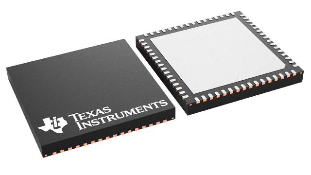
Packaging information
| Package | Pins VQFN (RGC) | 64 |
| Operating temperature range (°C) -40 to 85 |
| Package qty | Carrier 250 | SMALL T&R |
Features for the ADS42JB49
- Dual-Channel ADCs
- 14- and 16-Bit Resolution
- Maximum Clock Rate: 250 MSPS
- JESD204B Serial Interface
- Subclass 0, 1, 2 Compliant
- Up to 3.125 Gbps
- Two and Four Lanes Support
- Analog Input Buffer with High-Impedance Input
- Flexible Input Clock Buffer:
Divide-by-1, -2, and -4 - Differential Full-Scale Input: 2
VPP and 2.5 VPP
(Register Programmable) - Package: 9-mm × 9-mm VQFN-64
- Power Dissipation: 850 mW/Ch
- Aperture Jitter: 85 fS rms
- Internal Dither
- Channel Isolation: 100 dB
- Performance:
- fIN = 170 MHz at 2
VPP, –1 dBFS
- SNR: 73.3 dBFS
- SFDR: 93 dBc for HD2, HD3
- SFDR: 100 dBc for Non HD2, HD3
- fIN = 170 MHz at 2.5
VPP, –1 dBFS
- SNR: 74.7 dBFS
- SFDR:
89 dBc for HD2, HD3 and
95 dBc for Non HD2, HD3
- fIN = 170 MHz at 2
VPP, –1 dBFS
Description for the ADS42JB49
The ADS42JB69 and ADS42JB49 are high-linearity, dual-channel, 16- and 14-bit, 250-MSPS,
analog-to-digital converters (ADCs). These devices support the JESD204B serial interface with data
rates up to
3.125 Gbps. The buffered analog input provides uniform input impedance across a wide
frequency range while minimizing sample-and-hold glitch energy making it easy to drive analog
inputs up to very high input frequencies. A sampling clock divider allows more flexibility for
system clock architecture design.
The devices employ internal dither algorithms to provide excellent spurious-free
dynamic range (SFDR) over a large input frequency range.