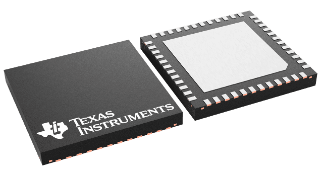
48-pin (RHS) package image

LMK04031BISQE/NOPB ACTIVE

Low-noise jitter cleaner with 1430 to 1570-MHz VCO:2 outputs for 2VPEC/LVPEC+LVDS+LVCOMS

ACTIVE custom-reels CUSTOM Custom reel may be available
open-in-new View alternates

Pricing

Qty Price
+

Additional package qty | Carrier options These products are exactly the same but come in a different carrier type

LMK04031BISQ/NOPB ACTIVE custom-reels CUSTOM Custom reel may be available
Package qty | Carrier 1,000 | SMALL T&R
Inventory
Qty | Price 1ku | +
LMK04031BISQX/NOPB ACTIVE custom-reels CUSTOM Custom reel may be available
Package qty | Carrier 2,500 | LARGE T&R
Inventory
Qty | Price 1ku | +

Quality information

Rating Catalog
RoHS Yes
REACH Yes
Lead finish / Ball material SN
MSL rating / Peak reflow Level-3-260C-168 HR
Quality, reliability
& packaging information

Information included:

  • RoHS
  • REACH
  • Device marking
  • Lead finish / Ball material
  • MSL rating / Peak reflow
  • MTBF/FIT estimates
  • Material content
  • Qualification summary
  • Ongoing reliability monitoring
View or download
Additional manufacturing information

Information included:

  • Fab location
  • Assembly location
View

Export classification

*For reference only

  • US ECCN: EAR99

Packaging information

Package | Pins WQFN (RHS) | 48
Operating temperature range (°C) -40 to 85
Package qty | Carrier 250 | SMALL T&R

Features for the LMK04031

  • Cascaded PLLatinum PLL Architecture
  • PLL1
  • Phase detector rate of up to 40 MHz
  • Integrated Low-Noise Crystal Oscillator Circuit
  • Dual redundant input reference clock with LOS
  • PLL2
  • Normalized [1 Hz] PLL noise floor of -224 dBc/Hz
  • Phase detector rate up to 100 MHz
  • Input frequency-doubler
  • Integrated Low-Noise VCO
  • Ultra-Low RMS Jitter Performance
  • 150 fs RMS jitter (12 kHz – 20 MHz)
  • 200 fs RMS jitter (100 Hz – 20 MHz)
  • LVPECL/2VPECL, LVDS, and LVCMOS outputs
  • Support clock rates up to 1080 MHz
  • Default Clock Output (CLKout2) at power up
  • Five dedicated channel divider and delay blocks
  • Pin compatible family of clocking devices
  • Industrial Temperature Range: -40 to 85 °C
  • 3.15 V to 3.45 V operation
  • Package: 48 pin LLP (7.0 x 7.0 x 0.8 mm)

  • Target Applications

  • Data Converter Clocking
  • Wireless Infrastructure
  • Networking, SONET/SDH, DSLAM
  • Medical
  • Military / Aerospace
  • Test and Measurement
  • Video

  • Description for the LMK04031

    The LMK04000 family of precision clock conditioners provides low-noise jitter cleaning, clock multiplication and distribution without the need for high-performance voltage controlled crystal oscillators (VCXO) module. Using a cascaded PLLatinum architecture combined with an external crystal and varactor diode, the LMK04000 family provides sub-200 femtosecond (fs) root mean square (RMS) jitter performance.

    The cascaded architecture consists of two high-performance phase-locked loops (PLL), a low-noise crystal oscillator circuit, and a high-performance voltage controlled oscillator (VCO). The first PLL (PLL1) provides a low-noise jitter cleaner function while the second PLL (PLL2) performs the clock generation. PLL1 can be configured to either work with an external VCXO module or use the integrated crystal oscillator with an external crystal and a varactor diode. When used with a very narrow loop bandwidth, PLL1 uses the superior close-in phase noise (offsets below 50 kHz) of the VCXO module or the crystal to clean the input clock. The output of PLL1 is used as the clean input reference to PLL2 where it locks the integrated VCO. The loop bandwidth of PLL2 can be optimized to clean the far-out phase noise (offsets above 50 kHz) where the integrated VCO outperforms the VCXO module or crystal used in PLL1.

    The LMK04000 family features dual redundant inputs, five differential outputs, and an optional default-clock upon power up. The input block is equipped with loss of signal detection and automatic or manual selection of the reference clock. Each clock output consists of a programmable divider, a phase synchronization circuit, a programmable delay, and an LVDS, LVPECL, or LVCMOS output buffer. The default startup clock is available on CLKout2 and it can be used to provide an initial clock for the field-programmable gate array (FPGA) or microcontroller that programs the jitter cleaner during the system power up sequence.

    Pricing

    Qty Price
    +

    Additional package qty | Carrier options These products are exactly the same but come in a different carrier type

    LMK04031BISQ/NOPB ACTIVE custom-reels CUSTOM Custom reel may be available
    Package qty | Carrier 1,000 | SMALL T&R
    Inventory
    Qty | Price 1ku | +
    LMK04031BISQX/NOPB ACTIVE custom-reels CUSTOM Custom reel may be available
    Package qty | Carrier 2,500 | LARGE T&R
    Inventory
    Qty | Price 1ku | +

    Carrier options

    You can choose different carrier options based on the quantity of parts, including full reel, custom reel, cut tape, tube or tray.

    A custom reel is a continuous length of cut tape from one reel to maintain lot- and date-code traceability, built to the exact quantity requested. Following industry standards, a brass shim connects an 18-inch leader and trailer on both sides of the cut tape for direct feeding into automated assembly machines. TI includes a reeling fee for custom reel orders.

    Cut tape is a length of tape cut from a reel. TI may fulfill orders using multiple strips of cut tapes or boxes to satisfy the quantity requested.

    TI often ships tube or tray devices inside a box or in the tube or tray, depending on inventory availability. We pack all tapes, tubes or sample boxes according to internal electrostatic discharge and moisture-sensitivity-level protection requirements.

    Learn more

    Lot and date code selection may be available

    Add a quantity to your cart and begin the checkout process to view the options available to select lot or date codes from existing inventory.

    Learn more