Packaging information
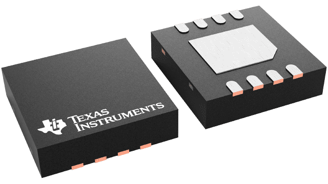
| Package | Pins WSON (DTK) | 8 |
| Operating temperature range (°C) -40 to 105 |
| Package qty | Carrier 3,000 | LARGE T&R |
Features for the OPA817
- Wide bandwidth:
- Gain-bandwidth product: 400 MHz
- Bandwidth (G = 1 V/V): 800 MHz
- Large-signal bandwidth (2 VPP): 250 MHz
- Slew rate: 1000 V/µs
- High precision:
- Input offset voltage: 250 µV (maximum)
- Input offset voltage drift: 3.5 µV/°C (maximum)
- Input voltage noise: 4.5 nV/√Hz
- Input bias current: 2 pA
- Low distortion (RL = 100 Ω,
VO = 2 VPP):
- HD2, HD3 at 10 MHz: –86 dBc, –100 dBc
- Supply range: 6 V to 12.6 V
- Supply current: 23.5 mA
- Shutdown current: 55 µA
- Performance upgrade to OPA656
Description for the OPA817
The OPA817 is a unity-gain stable, voltage-feedback operational amplifier for high-speed, high-precision and wide dynamic range applications.
The OPA817 has a low-noise junction gate field-effect transistor (JFET) input stage that features a wide gain-bandwidth of 400-MHz and a supply range from 6-V to 12.6-V. The fast slew rate of 1000-V/µs allows a wide large-signal bandwidth and low distortion when used as high impedance buffer in high-speed digitizers, active probes and other test and measurement applications.
The OPA817 offers extremely low input offset voltage of ±250-µV and offset voltage drift of ±3.5-µV/°C. The combination of pico-amperes of input bias current and low input voltage noise (4.5-nV/√Hz) makes the OPA817 an ideal wideband transimpedance amplifier in optical test and communication equipment as well as medical and scientific instrumentation.
The OPA817 is available in an 8-lead WSON package with an exposed thermal pad for heat dissipation. This device is specified to operate over the industrial temperature range of –40°C to +105°C.
.
.